The Apple G4 is a superscalar RISC microprocessor developed by Motorola. It is the next generation (4th generation to be exact, hence G4) PowerPC microprocessor and is meant to be a substantial improvement over the G3. To see specific improvements, please visit our Q&A section.
This site is meant to focus more on the architectural design of the G4--i.e. how the instructions are processed. Here is a detailed sketch of the MPC7400 Microprocessor:
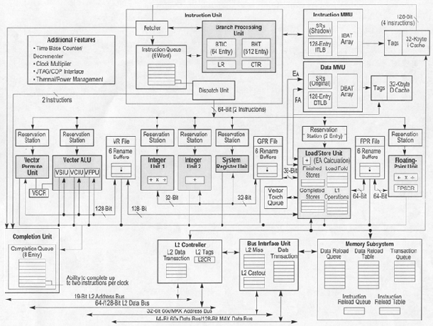
Note: The picture above is for the MPC7400, but there is also the MPC7410, MPC7440 and MPC7450. All these processors are considered G4 processors (as opposed to the G3, the MPC750), just each increasing number is a slightly "improved" model over the previous one. All use the same basic architecture, so here we use them interchangeably. For the most part, they will be referenced as a whole as the MPC74xx.
The G4 is superscalar, meaning it can fetch multiple instructions at once; four to be exact. As many as eight instructions can execute per clock and most instructions have a single clock-cycle execution time. The throughput is thus one instruction per clock cycle for most instructions.
Instructions in the MPC74xx are fetched sequentially by the fetcher and stored in a six-entry instruction queue, all part of the instruction unit (seen in the middle-top of the diagram). The dispatch unit then passes the instructions along to the correct execution unit.
The main execution units in the microprocessor are as follows:
- Floating point unit (FPU)
- Branch processing unit (BPU)
- System register unit (SRU)
- Load/store unit (LSU)
- Integer units (IUs)
- AltiVec units

As seen in the diagram the G4 has four stages through which all instructions pass. These stages are fetch, decode/dispatch, execute, and complete/write back. Also note that there are multiple stages in the execute stage depending on which unit is used -- i.e. the FPU is a 3 staged pipelined unit. The following is a break down of what each of the four basic stages does:
- Fetch
This stage involves the retrieving of instructions from memory and determining the location of the next instruction fetch. As stated earlier the BPU is wired to decode braches. - Dispatch
Much like Tomasulo's, the dispatch stage decodes the instruction from the fetch stage. This stage provides instrucitons with target destination a rename ID. If source operands are available then then execution is continued in the proper execution unit. Otherwise the stage will assign an ID to the register that will supply the operand when it is available. It will then wait until the renamed ID for each operands becomes available and then continue on to execution. - Execute
Instruction are dispatached to the proper functional units as seen in the above diagram. Two instructions can be dispatched per clock cycle. When the instruction is dispatched it is assigned to the completion queue. - Write Back/Complete
Once an instruction is completed it moves into this stage. Here execution results is transferred from the rename registers to the proper registers i.e. -- FPRs. Also if there an exception occurs in the logic, then the all following instructions are cancelled and execution results are discarded.
Floating Point Unit (FPU)
The floating point unit handles (surprise) all floating point operations, like fp add, subtract, multiply and divide. It is found on the far right, middle of the above diagram. It is a pipelined unit that has a latency of three cycles for single-precision operations. The pipelining allows one single- or double-precision instruction to be issued per clock cycle. The FPU contains thirty-two 64-bit floating-point registers to support these operations. Stalls due to resource contention are minimized by automatic allocation of six floating-point rename registers. Also, there is hardware support for denormalized numbers.
Branch Processing Unit (BPU)
Tells the instruction unit the address of the next instruction to be fetched. Please follow the link see our in depth section on the BPU.
System Register Unit (SRU)
The SRU is smack in the middle of the diagram. It is used for executing system-level instructions such as move to/from special-purpose register instructions. Instructions in the SRU are held for execution until all previously issued instructions have been executed (called execution-serialization) to maintain system state. The results of an SRU-executed instruction are not available for later instructions until the instruction completes (i.e. no forwarding).
Load/Store Unit (LSU)
The Load/store unit is a little to the left of the FPU and does what its name implies: it executes all load and store instructions, allowing for data transfer betwen cache/memory and the FPRs, GPRs and VRs (Floating point registers, integer registers and vector registers, respectively). While the load/store instructions are issued and decoded in program order, the actual memory accesses can occur out of order. Strict ordering, however, can be enforced using certain synchronizing instructions.
The LSU has its own dedicated adder and supports both big- and little- endian modes. Store instructions are executed with a throughput of one per cycle and a three-cycle total latency to the data cache. The actual time for a load or a store depends on whether the on-chip cache, the L2 cache, memory or disk is being accessed.
Integer Units (IUs)
There are two integer units, IU1 and IU2, found in the middle of the diagram near the SRU. The IU1 executes any integer instruction, while the IU2 can do most, losing the capability to do multiplication and division.
Each IU contains three single-cycle "subunits": and adder/comparator, a subunit for logical operations and one for performing rotate and shift operations. Only one subunit can be executing an instruction at a time. The IU1 also contains a 32-bit multiplier/divider.
AltiVec
The AltiVec instruction set architecture is an extenstion of the PowerPC architecture. Please follow the link to see our in depth section on AltiVec.
And after all this, we finally reach the. . .
Completion Unit (not CU, that's something else)
The completion unit is the final stage for an instruction; quite literally the instructions' retirement home. It is found in the bottom-left of the diagram. When an instruction is dispatched by the Dispatch Unit it is given a sequential spot in this 8-entry completion unit. The completion unit then tracks the instructions and "retires" them in correct program order. It also has the all-important job of flushing instructions from the mispredicted branch. These two jobs ensure in-order completion and correct recovery from a mispredicted branch. When an instruction is completed along with all instructions ahead of it, and there are no pending exceptions, the instruction is retired, that is, it is removed from the completion queue.
©2001, Eric Everstine & Linhong Zhang