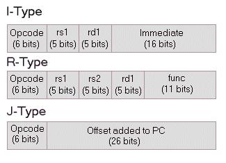
Instructions in DLX are 32 bit words which contain information describing the specific instruction type as well as the sources and destinations of data for that instruction. There are three instruction formats in the DLX architecture: R-type, I-type and J-type. The R-type format is used for instructions which use only reigsters, the I-type format is used for instructions which require immediate values and the J-type format is used for unconditional jump instructions. The instructions are all 32 bits in DLX and they are organized as follows
Note: The opcode consists of 6 bits which specify the exact instruction type. "rs" designates a source register and "rd" designates the destination register name (note that the ordering of source and desination registers is opposite of the machine code syntax). It takes five bits to name a register because there are 32 general purpose registers (GPRs).
Instruction types in more detail:
I-type: Contains the opcode, a source register name, a destination register name, and a 16-bit Immediate value. This instruction format is used for loads and stores, register-immediate ALU instructions, conditional branches, jump register and jump and link (linking saves the current PC in R31) register instructions.
R-type: Contains the opcode, two source register names, a destination register name and function bits. This instruction format is used for register-register ALU operations, reading/writing special registers and moves.
J-type: Contains the opcode, and a 26-bit immediate value. Only jump and jump and link instructions use this type.
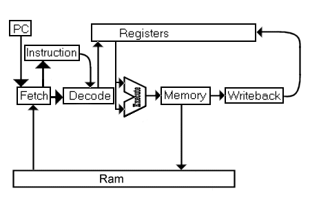
There are five stages of execution in the DLX architecture: Instruction Fetch (IF), Instruction Decode (ID), Execution (EX), Memory (MEM) and Write-Back (WB). Each stage takes as much time as the slowest one, even if it does not need this much time to complete. This time period is a clock cycle. Therefore, each instruction takes a total of 5 clock cycles from start to finish to execute. Each stage of execution corresponds to hardware in the cpu, as can be seen in the Figure 3.1 of Hennessy and Patterson. Each "section" of hardware along the data path can operate concurrently which pipelining takes advantage of to gain enourmous performance benefits.
Very specific operations are done in each stage.
1. Instruction Fetch (IR) - Read the instruction from memory and put it into the instruction register (IR). Update the new program counter (NPC) so that it points to the next instruction (PC + 4, or the next word in memory).
2. Instruction Decode (ID) - Decode the instruction (based on opcode). The output of registers (Regs[IR6..10]) and Regs[IR11..15]) from the register file is placed into temporary registers "A" and "B". Sign extend the portion of the instruction that could be an immediate value and put this value into temporary register "Imm".
3. Execution (EX) - What happens here depends on what type of instruction is being executed. The ALU is going to be operating in this cycle, performing the desired operation.
To handle floating point (FP) operations, DLX is extended to "Multicycle DLX". Multicyle DLX operation is very similar to normal DLX. The major conceptual change is in the EX stage.
Different floating point operations (add, multiply, divide, load/store) take different amounts of time to finish. They also take much more time then integer operations and use different hardware. This is why we have Multicycle DLX.
In short, we now have three additional funtional units to add to our Integer unit to be used in the EX stage. They are an FP/integer multiplier, an FP adder and an FP/integer divider. These units operate inbetween the ID and MEM stages, as does the normal EX stage which is extended to handle FP loads and stores as well. Each stage is itself divided into substages (with the exception of the divide stage) each taking a clock cycle (as you will learn this aids in pipelining So with mutlicycle DLX, the EX stage essentially becomes a variable-length, mutlicycle stage. Figure 3.44 in Hennessy and Patterson is a good visualization of Multicycle DLX.
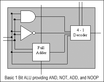
The Arithmetic and Logic Unit (ALU) is the single most important part of a CPU. It provides the hardware for all of the basic functions in a computer. The simple one bit ALU shown has 4 functions, AND, ADD, NOT, and NOOP. By calling these basic instructions from a microprogram, any operation can be performed.
Example:
Combine 8 of these ALUs by connecting the carry pins of the full adders and by joining the decoder inputs to a common bus. This simple modification makes a one byte CPU capable of 4 functions. Assume the following instructions are implemented NOOP (00 to the decoder), AND (01), NOT (10), and ADD (11). Implement the logical OR operation.
Answer:
C = OR A, B:
A' = NOT A Save the result of Not A
B' = NOT B Save Not B
C = AND A', B' AND the results, A' AND B' = A OR B (DeMorgan)
Real computers are not built from these bit-slice ALU chunks for several reasons such as the inherent difficulty in writing microcode and added time overhead of the microinstructions (OR takes 3 cycles). Despite this flaw, the microcode CPU is useful for explaining how an instruction is executed. Recall that an instruction has 5 stages of execution: Fetch, Decode, Execute, Memory, and Writeback. In the bit-slice CPU model, the program counter determines the next instruction, and it is fetched from memory, then the decode phase would select the microinstructions required to execute the instruction, the Execute phase would process each microinstruction, memory access would then occur, followed by a writeback to the main CPU registers.
Pipelining is a method in which computer manufacturers increase the throughput of their processors. This is accomplished by analyzing the steps that each instruction needs to go through in order to execute and finding a faster way to do it. In a pipeline, each of the five stages (described before) is transformed into a small, self contained mini CPU. On an integer pipeline, each unit can perfrom its individual task in one clock cycle, so after five clock cycles, one instruction is completed. An obvious question to ask at this point is, "Why is this useful, couldn't we complete an instruction in one clock cycle before?". The answer is yes, we have effectively made an instruction take 4 more cycles to complete, but we have shortened the time per clock cycle by approximately one fifth. Yielding a result of instructions taking the same amount of time to complete as before.
Now there's another obvious question, "So what?" All we've done at this point is to add a small bit of overhead to the entire
execution process, making it even more complicated. (This is the cool part) If we look at the time to complete a second
instruction, we'll see that it was fetched while the first instruction was decoded, and was finished on clock cycle 6! Using a
pipeline, we can increase the speed of execution by nearly 5 times!

Where does this 500% improvement come from? Looking at an unpipelined CPU, we see that there are five separate stages to execution, and each one must be performed sequentially. There can be no writeback until execution has completed because there's no data to write back yet. Computer designers noticed this and built a processor that would overcome this problem by a pipeline. Each part of the CPU is working on a different instruction.
In a perfect world, once the pipeline is going, an instruction will be completed every clock cycle, yeilding a CPI (Clock cycles Per Instruction) of 1. This never happens. Very rarely are instructions completely independent of each other. If instruction 2 needs the output of instruction one, then instruction 2 is going to have to wait. A more clear description of these Data Hazards is coming later in this document.
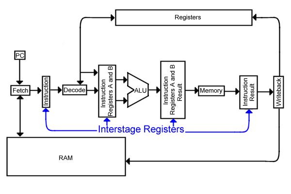
Clearly, the bookkeeping for the pipeline is more complex, otherwise each stage would forget which instruction is was processing, and then the entire machine would crash to a halt. On a single stage CPU, there is only one instruction to consider, therefore, there is only one instruction register and only one copy of the data registers. When expanding to a 5 stage pipe, each stage needs to have it's own copy of the instruction as well as it's own local image of the data registers. Designers do not want to build 5 complete register banks for each CPU, so the minimum of information is kept on hand for each stage. These local registers are placed between each stage in the CPU providing the vital transient information. Since there are 5 stages, 4 interstage registers are needed. Here's what they need to hold:
There isn't much data actually stored in the interstage registers, so their cost to performance enhancement ratio is excellant. The added time caused by these registers is very small. They can be built from simple "D" flip-flops using the trailing edge of the clock to latch. These registers are a major reason that 5 times the clock rate of the pipeline is larger than the clock rate of the single stage CPU.
Data hazards occur when an instruction needs the results of a previous instruction in the pipeline which has not been resolved yet. The instruction which needs data is unable to proceed until it obtains the required information and the pipeline is forced to stall to avoid the hazard which creates pipeline inefficiency. A simple example of a data hazard would be the following code segment:
LW   R1, 100(R2)
ADD  R3, R1, R4
The ADD instruction needs the result from the LW instruction (R1) before it has been written back the pipeline would proceed as follows (where ST indicates a stall):
     CC1 CC2 CC3 CC4 CC5 CC6 CC7 CC8
LW    IF  ID  EX MEM  WB
ADD       IF  ST  ST  ID  EX MEM  WB
Simple data stalls such as this one is easily overcome with forwarding. Multicycle DLX provides many more opportunities for data stalls due to the longer execution processes which may be required.
Data Hazards are classifed as RAW, WAR, and WAW Hazards.
Let's assume we have two instructions, x and y with x proceeding y.
RAW (Read after write) - y tries to read a source register before x writes to it. So x incorrectly gets the old value. RAW hazards are the most frequent type and forwarding is used to handle them
The example given in the previous section, What are data hazards? is a good example of a typical RAW hazard.
WAW (Write after write) - y tries to write to a register before x writes to it. The end result is the register retains the value given it by x which is incorrect, it should retain the value given it by the instruction latest in the pipeline, y. This happens frequently in the Multicycle DLX pipeling because of the instructions of varying lengths. This type of hazard is not as easy to overcome. It can be done with dynaming rescheduling and register renaming but that is out of the scope of this document.
Here is an example of a WAW hazard:

ADDF F1, F2, F3
LF F1, 100(R2)

      CC1 CC2 CC3 CC4 CC5 CC6 CC7 CC8 CC9
ADDF   IF  ID  A1  A2  A3  A4 MEM  WB
LF         IF  ID  EX MEM  ST  ST  ST  WB
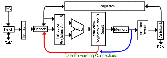
One solution to RAW hazards is called forwarding. In this method, the interstage registers for certain producer - consumer pairs are connected. In this way, whenever a result is calculated by an earlier instruction, the decode module can allow data to be used before the writeback stage records the result. The name Forward is used because data is passed to a later instruction (even though a diagram shows a backward arrow). Earlier, when describing RAW hazards, this example was presented:
     CC1 CC2 CC3 CC4 CC5 CC6 CC7 CC8
LW    IF  ID  EX MEM  WB
ADD       IF  ST  ST  ID  EX MEM  WB
when including forwarding, we can reduce the stalls like so:
     CC1 CC2 CC3 CC4 CC5 CC6 CC7 CC8
LW    IF  ID  EX MEM  WB
                     \    Forward the result from MEM to EX
ADD       IF  ID  ST  EX MEM  WB
Most stalls caused by data hazards can be removed by using forwarding, but the problems caused by loading may still require a hazard. A possible solution would be to reorder the code so loads are not directly preceding related instructions.
In addition to data hazards (which can be solved by forwarding), there are other types of hazards in a pipelined architecture. A Control Hazard is the name associated with any kind of branch. Branches are especially difficult for a hardware disigner to deal with because they are unpredictable (why would you put in a conditional branch is you always knew what the answer was?). Whenever an if statement is loaded into a pipeline, it is executed normally, but when does the Program Counter (PC) get updated? Once the PC is updated, that instruction must be executed. What happens to he instruction that was fetched after the branch, but before the target is known?
          CC1 CC2 CC3 CC4 CC5 CC6
BRANCH    IF  ID  EX MEM  WB
NEXT Line     IF  ID  EX MEM  WB     ???
The problem is solved in a number of ways: assuming a branch is taken (or not taken) and squashing the pipeline if it is invalid, or placing a Branch Delay Slot instruction after the branch that needs to be executed regardless of the outcome of the conditional. For more information, refer to the textbook or other tutorial web pages.
  I. How an instruction works
   1. Why do DLX instructions require 5 bits to name a register?
      What portion of a DLX instruction would contain an immediate value?
   2. Why does DLX use five different stages of equal duration?
      What determines the length of the stages?  What is this length of time called?
   3. What is the purpose of multicyle DLX?  What about it lends itself to pipelining?

 II. Pipelining
   4. How long does it take to execute 10 instrucions on an unpipeline CPU with CC time
      of 50 ns?  On a piplelined machine (10 ns per cycle)?  Compare the speedup by the
      pipeline with a 100 instruction mix.  Ignore all hazards.
   5. What parts of the instruction are really needed for each stage?
      Do we really need to keep the instruction in the MEM-WB interstage register?
      Why or why not?

III. Data Hazards
   6. Assuming no forwarding, do these instructions cause a stall?  Why or why not?
          LW  R1, 100(R2)
          ADD R2, R1, R3
     Is there any case where an ALU op following a load does not create a stall condition
     requiring handling?

   7. Give an example of both RAW and WAW hazards.  Why doesn't DLX have WAR hazards?
   8. How many stalls will be encountered in this code segment? What is the CPI? Assume
     Memory Reads and Writes can happen on the same clock cycle and there are separate
     Instruction and Data memories.

     LW   R1, 100(R0)
     LW   R2, 104(R0)
     ADDI R3, R0, #42
     LW   R4, 0(R3)
     XOR  R5, R1, R4
     ADD  R5, R2, R5

  9. Re-solve the previous code fragment with the structural hazards due to register
     contention and memory still in place (only one read per cycle).
 10. Re-solve the previous code fragment with forwarding, but no structural hazards.
1:
   Because there are 32 registers and 5^2=32 so 5 bits is enough to encode the reigster
   names. The last 16 bits of an I-tpye instruction.
2:
   So that it can later be pipelined efficiently.
   The stages are all as long as the slowest stage.
   This time period is called a clock cycle
3:
   Mutlicycle DLX exists so that floating point ops can be incorporated into DLX.
   The functional units are split up so they themselves can be pipelined.

4:
   On the unpipelined machine, 10 instructions are completed in 10 clock cycles. At 50
   ns per clock cycle, that if 500ns for completion. On the pipelined machine, 10
   instructions (no hazards) are completed in 14 clock cycles (there are 4 cycles
   wasted filling the pipe, and then they complete one per cycle, 4 + 10 = 14. 14
   cycles times 10 ns equals 140 ns. 500 ns / 140 ns = 3.57, so the speedup is 3.57.

   On the 100 instruction version, the unpipelined version takes (100 cycles x 50ns)
   5000 ns or 5 ms, while the pipeline takes (100 + 4 = 104 cycles X 10 ns) 1040 ns or
   1 .04 ms. 5 / 1.04 = 4.81, so the speedup is 4.81. Obviously, as the number of
   instructions goes to infinity, the speedup reaches 5.0. Too bad the hazards are
   really negligible.

5:
   I'm solving this backwards since the contents are cumulative.
   Memory - Writeback : The destination register number and the ALU result.
   Execute - Memory   : Destination register, the ALU result, the contents of the "A"
                        operand register (for SW operations), 2 bits to determine if
                        there is a memory operation (read or write) or not.
   Decode - Execute   : Operands "A" and "B", the full instruction except for the name
                        of register "A".
   Fetch - Decode     : Full instruction (that's it)

   The insrtuction is unnecessary for the last interstage register because the MEM
   cycle can set the destination address to R0 if there is no writeback. ;)
6:
   Yes.  ADD requires R1 in the ID stage and LW doesnt produce it until WB.
   No, ALU ops following Loads always create a stall condition.
7:
   RAW:   LW  R1, 100(R2)   WAW:  DIVF F1, F2, F3
          ADD R2, R1, R3          ADDF F1, F4, F5
   WAR hazards are not a problem in DLX because the registers are always
   read from early and written to late.
8:
| Insrtuction | 1 | 2 | 3 | 4 | 5 | 6 | 7 | 8 | 9 | 10 | 11 | 12 | 13 | 14 | 15 | 16 |
| LW R1, 100(R0) | IF | ID | Ex | Mem | WB | |||||||||||
| LW R2, 104(R0) | IF | ID | Ex | Mem | WB | |||||||||||
| ADDI R3, R0, #42 | IF | ID | Ex | Mem | WB | |||||||||||
| LW R4, 0(R3) | IF (2 Stalls) | ID | Ex | Mem | WB | |||||||||||
| XOR R5, R1, R4 | IF (2 Stalls) | ID | Ex | Mem | WB | |||||||||||
| ADD R5, R2, R5 | IF (2 Stalls) | ID | Ex | Mem | WB | |||||||||||
In this problem, Writeback and Decode can occur simultaneously because of the assumption of two cycle registers. Fetch and Memory can happen at the same time because of split memories. The dependencies on the previous instructions are the only cause of the 6 stalls. Given the six instructions and the 16 clock cycles required, the CPI is 2.67.
| Insrtuction | 1 | 2 | 3 | 4 | 5 | 6 | 7 | 8 | 9 | 10 | 11 | 12 | 13 | 14 | 15 | 16 | 17 | 18 | 19 | 20 | 21 | 22 |
| LW R1, 100(R0) | IF | ID | Ex | Mem | WB | |||||||||||||||||
| LW R2, 104(R0) | IF | ID | Ex | Mem | WB | |||||||||||||||||
| ADDI R3, R0, #42 | IF (3 Stalls) | ID | Ex | Mem | WB | |||||||||||||||||
| LW R4, 0(R3) | IF (3 Stalls) | ID | Ex | Mem | WB | |||||||||||||||||
| XOR R5, R1, R4 | IF (3 Stalls) | ID | Ex | Mem | WB | |||||||||||||||||
| ADD R5, R2, R5 | IF (3 Stalls) | ID | Ex | Mem | WB | |||||||||||||||||
In this variation, Writeback and Decode as well as Fetch and Memory are mutually exclusive pairs, so another stall is needed for each occurance. There are 12 stalls. Given the six instructions and the 22 clock cycles required, the CPI is 3.67. Notice that this horribly inefficient pipeline is still faster than the original 5 cycle non-pipelined CPU.
| Insrtuction | 1 | 2 | 3 | 4 | 5 | 6 | 7 | 8 | 9 | 10 | 11 |
| LW R1, 100(R0) | IF | ID | Ex | Mem | WB | ||||||
| LW R2, 104(R0) | IF | ID | Ex | Mem | WB | ||||||
| ADDI R3, R0, #42 | IF | ID | Ex | Mem | WB | ||||||
| LW R4, 0(R3) | IF | ID | Ex | Mem | WB | ||||||
| XOR R5, R1, R4 | IF | ID, Stall | Ex | Mem | WB | ||||||
| ADD R5, R2, R5 | IF, Wait | ID | Ex | Mem | WB | ||||||
This final variation is awesome. The data dependencies from before are nearly obliterated! The LW causes a stall because a valid result is not known until after the memory cycle. Notice how the stall propigates down the pipeline. This is because the Decoder is busy stalling on the XOR, so the ADD can't be pushed from the Fetcher to the Decoder. There are two stalls in this scheme. The six instructions and 11 clock cycles makes the CPI 1.83. If this pipe were run on a long, branch-free code segment, it will limit to very close to 1 (probably 1.1 or so due to the LW stall).