
![]()
Purpose of this document:
You're a smart PC consumer, or perhaps even aim to be a smart computer architect. You've read the excellent cache review by another former Hugue-ian student covering the generals of cache theory Hennessy and Patterson style. But you're still aching for a few of the details - Sure cache is faster than main memory, but how is this accomplished? How do we construct cache memory? What are burst writes and wait states? Can we cover a few of the techniques H&P use to speed up caches in a little more detail? Have you been plagued by these and more questions? Woken up in the middle of the night in cold sweats wondering whether you could be the next "victim" of a victim cache? Well, fear not - the following document should allay those fears and have you back to sleeping through the night, my friend... And now here we go, right on with the show... get ready to impress your friends and confound your enemies!
Section 1 - Physical Cache Construction / Differences in Technologies
What
is cache?
How is cache
physically constructed?
What is a burst
write?
What is pipeline
burst SRAM (PB SRAM)?
What is the
difference between interleaved and linear burst modes?
What is this
"2-1-1-1" notation I keep seeing?
What is a wait
state?
What is the
difference between synchronous and asynchronous SRAM?
What is
Flow-Thru SRAM?
What is "No
Bus Latency" or "Zero Bus Turnaround" SRAM?
What is COASt?
What is
"Transactional" or "Non-blocking cache"?
What is
motherboard / daughterboard / integrated cache?
How do I find
out what kind of cache I have in my machine?
Section 2 - Speeding up Caches, H&P-style
The great
cache performance formula
Reducing
miss rate:
One Technique For Reducing Conflict Misses - Victim
Caches
One Technique for Reducing Compulsory Misses - Instruction
Prefetching
Reducing
hit time:
Small and Simple Caches
Pipelining Writes
Reducing
miss penalty:
Sub-block Placement
Early Restart and Critical Word First
Section 3 - Cache Questions
Cache
Questions and Answers
Section 1 - Physical Cache Construction / Differences in Technologies
What is cache?
Cache memory is a small block of very high-speed RAM where recently read blocks of memory
are stored. Conceptually, the idea is to try to guess what chunk the currently
running program will next request and provide that chunk as quickly as
possible. Remembering the memory hierarchy, we want
to place recently-accessed memory chunks in fast memory residing as close as possible to
the processor, reducing costly runs out to slow main memory.
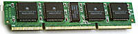
How is cache physically constructed?
L1
cache [Hell of Caches] is the smaller, faster, more expensive cache (typical size is
about 16 - 32k, operating at processor speed) located onboard the processor. This
on-chip location gives an immediate speed advantage to L1 since it can talk directly to
the processor without having to send signals across the bus lines. Due to the
location of L1 cache, it is often referred to as "internal cache", while L2 is
often referred to as "external cache" (since it is generally located off-chip
and must communicate with the CPU through bus lines). Watch this carefully, however
-- newer Pentium chips incorporate L2 cache onboard the CPU as well, making this
"internal/external" terminology somewhat dated.
L2
cache [Hell of Caches] is typically constructed using SRAM (Static Random
Access Memory) modules. SRAM runs faster than DRAM (the type of module typically used for main memory)
due to several reasons. The first is that bits stored in SRAM remain there
"statically" until power down or alteration (hence the name) without having to
be refreshed periodically like DRAM. Additionally, certain types of SRAM are able to
synchronize themselves with the CPU better than regular RAM, thus reducing wait states (see below). These differences are significant; SRAM
has a typical access time of 8-12 ns while most DRAM takes about 50-60 ns. As with
all elements in this crazy world of computers, we've sacrificed something to gain this
performance leap. In this case, we're gonna have to pony up a few more bucks per
byte - SRAM modules have more transistors than DRAM modules (necessary to provide the
"no-need-to-refresh" nature of the chips), and are therefore more expensive to
manufacture. Still hungry for even more technical specs on this stuff including SRAM
pinouts and timing diagrams? Check out IBM Microelectronics' Understanding
SRAM Operation.
Normally, data writes occur throughout the computer at a set rate, sharing bus bandwidth with all other processes. During a burst write, however, the computer gives full control of the hardware over to memory. The computer's bus is basically reserved for transfer of a short "burst" of data, allowing transfer rates to jump far above normal levels. These burst writes must be short, however, as it is difficult to reserve the bus for very long and not cause perceptible performance losses in other areas.
What is pipeline burst SRAM (PB SRAM)?
Pipeline burst SRAM uses pipelining techniques to execute SRAM requests in parallel, speeding up multiple accesses to the SRAM modules and removing some of the burden on the bus.
What is the difference between interleaved and linear burst modes?
When bursting SRAM goes to access data, it includes logic to allow it to cycle through the addresses by itself without any help from the CPU. Intel machines require that this addressing be "interleaved" (i.e., access addresses 0, 2, 4, 6, ... on the first pass and 1, 3, 5, 7, ... on the second pass). PowerPC and other machines require that this addressing be "linear" (i.e., access addresses 0, 1, 2, 3, ...).
What is this "2-1-1-1" notation I
keep seeing?
This refers to the number of clock cycles which "bursting" cache
requires to access data. It's often listed in formats such as "2-1-1-1" or
"3-2-2-2". The first number indicates the number of clock cycles required
to deliver the first data chunk, the second indicates the number of clock cycles required
for the second data chunk, etc.
Typically, your computer processor is running much faster than your main system memory (assumed to be DRAM). This causes problems because the processor has to slow itself down to communicate with the DRAM. It's like having a fast-talking used-car salesman babbling at a slow, drawling Texan - the salesman's gonna have to slow himself down if he's going to connect with this guy and unload a Kia Sportage (fat chance). So the processor does just that, slowing communication down by giving up clock cycles to other processes while it waits for the slower DRAM to catch up. These sacrificed clock cycles are termed "wait states". The benefit synchronous SRAM has over asynchronous SRAM and traditional DRAM in this category is that it is able to match the system clock much more closely, reducing or even eliminating wait states all together.
What is the difference between synchronous and asynchronous SRAM?
Asynchronous and synchronous refer to whether the SRAM modules have their communications synchronized to match the processor (synchronous = "we're in tune with the processor", asynchronous = "we're not in tune with the processor"). Referring to the previous section, "asynchronous" SRAM can introduce wait states into data transfers. Even with the penalty of taking on these wait states, a hit on an asynchronous cache module still beats the heck out of having to trot out to our oh-so-slow DRAM to grab data. All things being equal, though, take the synchronous SRAM if you can get it.
In Flow-Thru SRAM, all necessary control signals for a given operation are prepared before the timing clock inside the chip fires. This allows the SRAM module to quickly crank data out the other side, effectively completing the data transfer stage in less than one clock cycle.
What is "No Bus Latency" or "Zero Bus Turnaround" SRAM?
When switching between READ and WRITE modes, standard synchronous pipelined burst SRAM requires a blank processor cycle (or "NOP" - no operation) to perform the switch over. This additional latency has been the target of several companies, who have all created their own proprietary solutions for eliminating the NOP and thus speeding up cache access. Cypress Semiconductor offers "No Bus Latency" SRAM, while Micron offers "Zero Bus Turnaround" (or "ZBT") SRAM. Various other companies likely offer similar modules under different names, but they all accomplish essentially the same task. Really interested in how many cycles can be saved by eliminating this latency? Here's the table Micron offers lauding the praises of their ZBT SRAM (table source). This table gives the type of SRAM and the minimum number of cycles required for a READ-WRITE-READ combination:
| SRAM | Number of Cycles |
|---|---|
| Pipelined SyncBurst | 7 |
| Pipelined ZBT | 5 |
| Flow-Thru SyncBurst | 5 |
| Flow-Thru ZBT | 4 |
COASt stands for "Cash On A Stick". Yeah, I thought they were kidding at first, too. COASt is an older Intel specification for how PB SRAM in the L2 cache should be constructed to integrate tightly with other Intel hardware. COASt-compliant memory modules are on cards that plug into CELP ("Card Edge Low Profile") slots in the system's motherboard. There are multiple revisions of COASt (I was able to find information on revisions from 1.3 - 2.1, and there may be even more recent revisions). I'm not really gonna get into this, so if you want to get more info on COASt, check out Intel or the IBM chip notes.
What is "Transactional" or "Non-blocking cache"?
Typically, caches can only handle one request for data at a time. If data is not found within the cache during a request for information (a "miss"), then the data is fetched from main memory. During this data fetch, the cache is usually "blocked", meaning that no other cache requests are allowed to occur. In "non-blocking caches", however, this is not the case. Rather than sit idly by twiddling its thumbs waiting for the miss to be filled from DRAM, the cache takes more requests from the processor and attempts to fill them.
This technique has been incorporated by Intel into the L2 cache in their newer Pentium Pro and Pentium II machines. Success of this scheme required another recent Intel innovation -- the "Dual Independent Bus (DIB)" scheme which provides a high-speed "backside bus" connecting the L2 cache directly to the processor (rather than using the slower standard memory bus).
What is motherboard / daughterboard / integrated
cache?
These all refer to different placement of the L2 chips. In motherboard cache, the L2
cache is made up of chips which are soldered directly onto the motherboard. The idea
with COASt was to provide a similar type of cache, but
in a plug-in form which allowed the cache to be easily removed and upgraded.
Motherboard cache and COASt modules both represent older, slower cache solutions which
must use the standard memory bus to transfer data. More recent Intel machines use a
"daughterboard" which plugs directly into the motherboard, allowing the cache to
run at half the processor speed and still retain the uprgradeability COASt offered.
Finally, the most recent Intel chips include an integrated L2 cache, where the L2 cache is
actually located directly on the CPU, thus allowing it to run at full processor speeds.
How do I find out what kind of cache I have in my machine?
Well, this will require taking apart your machine and using a magnifying glass to inspect the tiny print on the L2 cache chip. Ha! Foolish mortal! You've probably already got a screwdriver and a magnifying glass, don't you?! We're computer science students - we don't TOUCH HARDWARE!! You had to know we'd have a slightly more clever way of doing things. The programs listed below should give you a nice insight into your machine's caching strategy and chip sizes without straining your precious eyesight. Standard software caveat - I'm making no personal guarantee that these programs will do anything useful, or that they won't completely screw your machine. Take precautionary measures (i.e., do a virus check) with all software, everything from these downloaded utilities to shrink-wrapped stuff you bought from that guy Zeke at Computer City.
| Program | Purpose |
Author |
|---|---|---|
| Cachet | Identify write strategy of your PC's cache. | Intel |
| CCT386 | Shows how good a fit your main memory configuration is for your cache configuration. | OverByte |
| Nucache | Reports CPU and external bus speed, L1 and L2 cache sizes (program reportedly flaky). | Nutek Memories |
| CACHCHK | Check out sizes/speeds of L1 and L2 caches. | Ray Van Tassle |
Section 2 - Speeding Up Caches, H&P Style
The great cache performance formula:
[Average memory access time = Hit time + (Miss rate * Miss penalty)]
As well will see, all of Hennessy and Patterson's schemes to speed up memory access using caches involve manipulating one of the three variables above. Hit time represents the number of nanoseconds it takes to access data if it is found in the cache. Miss penalty is the number of nanoseconds required to trot out to main memory and bring in the requested data when the address we want is not located in the cache. Miss rate represents the average percentage of data requests to the cache which result in "misses" when the address we want is not stored in the cache.
The following three sections will give a breakdown by variable with a detailed description of two techniques H&P discuss for improving each variable.
There are three main types of misses which affect caches: "compulsory", "capacity", and "conflict". I will briefly explain all three, then give examples of how we can reduce two of these miss problems.
One Technique For Reducing Conflict Misses - Victim Caches:
A "victim cache" is sort of a safety-net for another cache, catching discarded elements as they leave the cache. When a miss occurs to an address in cache memory, the data in that address is typically discarded from cache memory and filled with the new data. Now, pretend that we again need to access the block we just discarded. We have to throw out the data we just got and make another costly run out to main memory to get back the data. This process can get somewhat time consuming if two blocks are constantly fighting over the same cache location! To solve this problem, "victim caches" were invented...
Imagine that your mom has a bad habit of throwing out your stuff (like that favorite baseball hat that you took so long to break in!). Every time she throws something out, you have to drive half an hour out to the dump and search for it. Sick of this, you create a "trash box". Anything that your mom wants to throw out first goes into the "trash box". Once the trash box is filled, any item can be thrown in the garbage to go to the dump. If you want something bad enough, you'll get it out of the trash box in time or you're stuck running out to the dump to search for it.
The trash box in this little story represents the victim cache in a computer. The victim cache sits between the normal cache and main memory. As blocks map into non-empty slots in cache memory, the blocks in the cache are removed to make room. However, instead of just letting the data disappear into the ether as we would normally do, these "victim" blocks are sent down to the victim cache. Now, when a miss occurs, we can consult the victim cache to see if it perhaps holds the address we want before making a costly trot out to main memory.
One Technique for Reducing Compulsory Misses - Instruction Prefetching:
With prefetching, the idea is to go grab the next piece of data which the processor will request and place it in the cache (or in some sort of quickly-accessed buffer) to cut down on compulsory misses. That way, even if no previous instructions have touched the memory block which must be accessed next, there's still a chance we'll get a cache hit. Imagine if they had psychics working at the deli counter in the dining hall -- on your way to the dining hall, the psychics could read your mind and figure out the sandwich you wanted, which would be ready for pickup when you got there. Wow! No more waiting in lines! Well, that's the idea, but the processor doesn't need to make a 1-900 call to Diane Warwick to guess the next chunk of data to grab -- it uses hardware prefetching and compiler-controlled prefetching techniques to permit proper prognostication (whew! try that one three times fast!).
Hardware prefetching involves guessing the next consecutive chunk
which will be required by the cache. In the example H&P give in their book, a
miss to cache causes two blocks to be fetched -- the one which we wanted and couldn't find
in the cache (the "requested" block) PLUS the next consecutive block in memory
(the "prefectched" block). The requested block gets assigned to its place
in the cache, while the prefetched block is thrown into a buffer. When the cache is
operating and a "miss" occurs, the processor first checks this buffer to see if
it contains the block requested before running out to main memory.
Compiler-controlled prefetching involves allowing the compiler to slip special prefetch instructions into your code which let the machine know ahead of time that it can begin loading a chunk of data into the cache. This technique is useful in reducing the number of unnecessary prefetches which can occur with hardware prefetching techniques. However, it should be noted that prefetching of this sort requires a non-blocking cache so execution can continue while data is being prefetched into the cache.
When we actually do manage to get a hit out of the cache, it still takes a certain amount of time to locate and access the data within the cache. Here, I will review two of H&P's techniques for reducing this time.
Small and simple caches is a recommendation to
the cache to designer to keep the cache relatively small and uncomplex. By building
a small cache, less address tags need to be checked to determine whether a hit has
occurred. By keeping the structure and organization techniques simple (H&P
recommend using a direct-mapped
cache [Hell of Caches] if possible), more operations can be squeezed into a single
clock cycle.
Pipelining writes involves organizing write hits to cache so they can be performed in parallel. The difficulty in doing this is that we need to know whether a tag is in the cache before we allow the data to go ahead and write itself. How is this accomplished? The tag detection and data writing are split into two separate units and run in parallel. This way, we avoid having to wait for tag detection to complete before writing data into the cache. Though we are always "one write behind", so to speak, the overall speedup is much greater using this pipelining technique.
| Time 1 | Time 2 |
Time 3 |
|---|---|---|
| is tag 1 in cache? | if tag 1 found, write data | |
| is tag 2 in cache? | if tag 2 found, write data | |
| is tag 3 in cache? ... |
Reducing Miss Penalty:
Inevitably, we will occasionally have a cache miss. When this occurs,
a "penalty" is paid in clock cycles which would have been avoided if the data
had been in the cache. Even if this penalty can be reduced by one clock cycle, that
cycle will be saved every time a cache miss occurs. Two techniques H&P cover for
reducing miss penalty have already been mentioned briefly: second
level caches [Hell of Caches] and non-blocking
caches. Don't worry, I wouldn't try to rip you off -- I'll be covering two of
the other H&P solutions for reducing miss penalty.
Sub-block placement is a technique which
allows you to take advantage of large cache blocks while still retaining low miss
penalties. Large blocks are advantageous to the cache designer because they tend to
cut down the number of tags which must be checked, thus reducing hit time. The same
overall amount of information can be stored; we just need fewer tags to represent
it. The problem is that large blocks tend to increase miss penalty -- when a miss
occurs, these larger blocks take a long time to stuff into their location in the cache.
One solution presented in the text is "sub-block placement". In this
technique, each of the large blocks is divided up into "sub-blocks" of smaller
size. Now, instead of reading in each full block every time we get a miss, we can
just read in the sub-block. Each sub-block gets a "valid" bit to indicate
whether it contains usable data. So now be careful -- when we request a sub-block
and check the cache for a hit on that sub-block, the existence of a matching tag on a
large block doesn't necessarily mean we've got a hit! We need to check the
sub-block's matching "valid" bit to make sure the data is good.
The idea here is that we've managed to simulate smaller blocks within this large block
scheme. Instead of giving each sub-block its own entire tag, the "valid"
bit suffices as a poor man's tag. We're able to take advantage of the reduced hit
times that come with large blocks while still retaining the low miss penalties of small
blocks.
Early restart and critical word first
are two techniques which allow the processor to get back to what it's doing a little
quicker than usual when using a large block scheme. Large blocks are often
multi-word, but the important observation required for these two techniques is that the
processor generally only deals with single words in any given instruction. So
really, the miss that sparked this cache fill was probably just a miss of one single word.
Early restart takes advantage of this fact by watching the block
in cache fill up, word by word. When the word we requested which sparked the cache
fill arrives, we grab the word and give it to the processor. The processor then
completes the instruction execution and moves on to the next instruction. The whole
time, the block continues to fill up in the "background".
Critical word first takes advantage of the fact that the processor
probably only wants a single word by signaling that it wants the missed word to appear
first in the block. We receive the first word in the block (the one we actually
need) and pass it on immediately to the CPU which continues execution. Again, the
block continues to fill up in the "background".
- This page (c)
1998, Brian Renn -- last modified: 12/12/98 -
Permission is granted for reuse and distribution of unmodified page for
academic purposes.
Send non-academic permission requests and corrections to brenn@glue.umd.edu.