8 Execution of a Complete Instruction – Datapath Implementation
Dr A. P. Shanthi
The objectives of this module are to discuss how an instruction gets executed in a processor and the datapath implementation, using the MIPS architecture as a case study.
The characteristics of the MIPS architecture is first of all summarized below:
• 32bit byte addresses aligned – MIPS uses 32 bi addresses that are aligned.
• Load/store only displacement addressing – It is a load/store ISA or register/register ISA, where only the load and store instructions use memory operands. All other instructions use only register operands. The addressing mode used for the memory operands is displacement addressing, where a displacement has to be added to the base register contents to get the effective address.
• Standard data types – The ISA supports all standard data types.
• 32 GPRs – There are 32 general purpose registers, with register R0 always having 0.
• 32 FPRs – There are 32 floating point registers.
• FP status register – There ia floating point status register.
• No Condition Codes – MIPS architecture does not support condition codes.
• Addressing Modes – The addressing modes supported are Immediate, Displacement and Register Mode (used only for ALU)
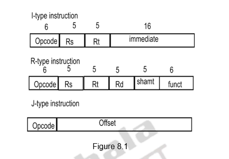
3 fixed length formats – There are 3 32-bit instruction formats that are supported. They are shown below in Figure 8.1.
We will examine the MIPS implementation for a simple subset that shows most aspects of implementation. The instructions considered are:
- The memory-reference instructions load word (lw) and store word (sw)
- The arithmetic-logical instructions add, sub, and, or, and slt
- The instructions branch equal (beq) and jump (j) to be considered in the end.
This subset does not include all the integer instructions (for example, shift, multiply, and divide are missing), nor does it include any floating-point instructions. However, the key principles used in creating a datapath and designing the control will be illustrated. The implementation of the remaining instructions is similar. The key design principles that we have looked at earlier can be illustrated by looking at the implementation, such as the common guidelines, ‘Make the common case fast’ and ‘Simplicity favors regularity’. In addition, most concepts used to implement the MIPS subset are the same basic ideas that are used to construct a broad spectrum of computers, from high-performance servers to general-purpose microprocessors to embedded processors.
When we look at the instruction cycle of any processor, it should involve the following operations:
- Fetch instruction from memory
- Decode the instruction
- Fetch the operands
- Execute the instruction
- Write the result
We shall look at each of these steps in detail for the subset of instructions. Much of what needs to be done to implement these instructions is the same, independent of the exact class of instruction. For every instruction, the first two steps of instruction fetch and decode are identical:
- Send the program counter (PC) to the program memory that contains the code and fetch the instruction
- Read one or two registers, using the register specifier fields in the instruction. For the load word instruction, we need to read only one register, but most other instructions require that we read two registers. Since MIPS uses a fixed length format with the register specifiers in the same place, the registers can be read, irrespective of the instruction.
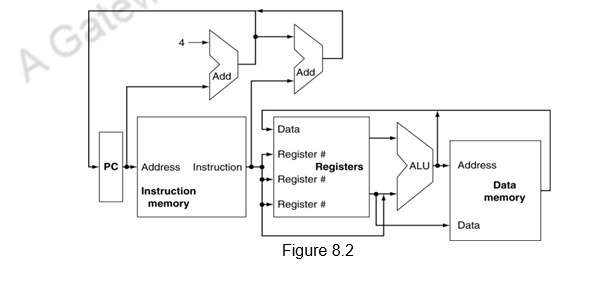
After these two steps, the actions required to complete the instruction depend on the type of instruction. For each of the three instruction classes, arithmetic/logical, memory-reference and branches, the actions are mostly the same. Even across different instruction classes there are some similarities. For example, all instruction classes, except jump, use the arithmetic and logical unit, ALU after reading the registers. The load / store memory-reference instructions use the ALU for effective address calculation, the arithmetic and logical instructions for the operation execution, and branches for condition evaluation, which is comparison here. As we can see, the simplicity and regularity of the instruction set simplifies the implementation by making the execution of many of the instruction classes similar. After using the ALU, the actions required to complete various instruction classes differ. A memory-reference instruction will need to access the memory. For a load instruction, a memory read has to be performed. For a store instruction, a memory write has to be performed. An arithmetic/logical instruction must write the data from the ALU back into a register. A load instruction also has to write the data fetched form memory to a register. Lastly, for a branch instruction, we may need to change the next instruction address based on the comparison. If the condition of comparison fails, the PC should be incremented by 4 to get the address of the next instruction. If the condition is true, the new address will have to updated in the PC. Figure 8.2 below gives an overview of the CPU.
However, wherever we have two possibilities of inputs, we cannot join wires together.
We have to use multiplexers as indicated below in Figure 8.3.
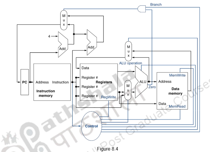
We also need to include the necessary control signals. Figure 8.4 below shows the datapath, as well as the control lines for the major functional units. The control unit takes in the instruction as an input and determines how to set the control lines for the functional units and two of the multiplexors. The third multiplexor, which determines whether PC + 4 or the branch destination address is written into the PC, is set based on the zero output of the ALU, which is used to perform the comparison of a branch on equal instruction. The regularity and simplicity of the MIPS instruction set means that a simple decoding process can be used to determine how to set the control lines.
Just to give a brief section on the logic design basics, all of you know that information is encoded in binary as low voltage = 0, high voltage = 1 and there is one wire per bit. Multi-bit data are encoded on multi-wire buses. The combinational elements operate on data and the output is a function of input. In the case of state (sequential) elements, they store information and the output is a function of both inputs and the stored data, that is, the previous inputs. Examples of combinational elements are AND-gates, XOR-gates, etc. An example of a sequential element is a register that stores data in a circuit. It uses a clock signal to determine when to update the stored value and is edge-triggered.
Now, we shall discuss the implementation of the datapath. The datapath comprises of the elements that process data and addresses in the CPU – Registers, ALUs, mux’s, memories, etc. We will build a MIPS datapath incrementally. We shall construct the basic model and keep refining it.
The portion of the CPU that carries out the instruction fetch operation is given in Figure 8.5.
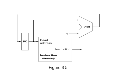
As mentioned earlier, The PC is used to address the instruction memory to fetch the instruction. At the same time, the PC value is also fed to the adder unit and added with 4, so that PC+4, which is the address of the next instruction in MIPS is written into the PC, thus making it ready for the next instruction fetch.
The next step is instruction decoding and operand fetch. In the case of MIPS, decoding is done and at the same time, the register file is read. The processor’s 32 general-purpose registers are stored in a structure called a register file. A register file is a collection of registers in which any register can be read or written by specifying the number of the register in the file.
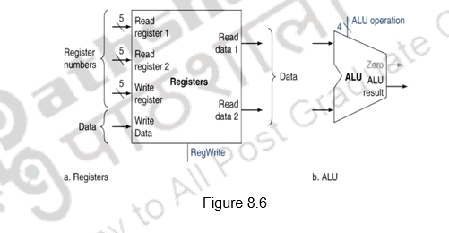
The R-format instructions have three register operands and we will need to read two data words from the register file and write one data word into the register file for each instruction. For each data word to be read from the registers, we need an input to the register file that specifies the register number to be read and an output from the register file that will carry the value that has been read from the registers. To write a data word, we will need two inputs- one to specify the register number to be written and one to supply the data to be written into the register. The 5-bit register specifiers indicate one of the 32 registers to be used.
The register file always outputs the contents of whatever register numbers are on the Read register inputs. Writes, however, are controlled by the write control signal, which must be asserted for a write to occur at the clock edge. Thus, we need a total of four inputs (three for register numbers and one for data) and two outputs (both for data), as shown in Figure 8.6. The register number inputs are 5 bits wide to specify one of 32 registers, whereas the data input and two data output buses are each 32 bits wide.
After the two register contents are read, the next step is to pass on these two data to the ALU and perform the required operation, as decided by the control unit and the control signals. It might be an add, subtract or any other type of operation, depending on the opcode. Thus the ALU takes two 32-bit inputs and produces a 32-bit result, as well as a 1-bit signal if the result is 0. The control signals will be discussed in the next module. For now, we wil assume that the appropriate control signals are somehow generated.
The same arithmetic or logical operation with an immediate operand and a register operand, uses the I-type of instruction format. Here, Rs forms one of the source operands and the immediate component forms the second operand. These two will have to be fed to the ALU. Before that, the 16-bit immediate operand is sign extended to form a 32-bit operand. This sign extension is done by the sign extension unit.
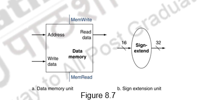
We shall next consider the MIPS load word and store word instructions, which have the general form lw $t1,offset_value($t2) or sw $t1,offset_value ($t2). These instructions compute a memory address by adding the base register, which is $t2, to the 16-bit signed offset field contained in the instruction. If the instruction is a store, the value to be stored must also be read from the register file where it resides in $t1. If the instruction is a load, the value read from memory must be written into the register file in the specified register, which is $t1. Thus, we will need both the register file and the ALU. In addition, the sign extension unit will sign extend the 16-bit offset field in the instruction to a 32-bit signed value. The next operation for the load and store operations is the data memory access. The data memory unit has to be read for a load instruction and the data memory must be written for store instructions; hence, it has both read and write control signals, an address input, as well as an input for the data to be written into memory. Figure 8.7 above illustrates all this.
The branch on equal instruction has three operands, two registers that are compared for equality, and a 16-bit offset used to compute the branch target address, relative to the branch instruction address. Its form is beq $t1, $t2, offset. To implement this instruction, we must compute the branch target address by adding the sign-extended offset field of the instruction to the PC. The instruction set architecture specifies that the base for the branch address calculation is the address of the instruction following the branch. Since we have already computed PC + 4, the address of the next instruction, in the instruction fetch datapath, it is easy to use this value as the base for computing the branch target address. Also, since the word boundaries have the 2 LSBs as zeros and branch target addresses must start at word boundaries, the offset field is shifted left 2 bits. In addition to computing the branch target address, we must also determine whether the next instruction is the instruction that follows sequentially or the instruction at the branch target address. This depends on the condition being evaluated. When the condition is true (i.e., the operands are equal), the branch target address becomes the new PC, and we say that the branch is taken. If the operands are not equal, the incremented PC should replace the current PC (just as for any other normal instruction); in this case, we say that the branch is not taken.
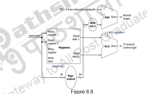
Thus, the branch datapath must do two operations: compute the branch target address and compare the register contents. This is illustrated in Figure 8.8. To compute the branch target address, the branch datapath includes a sign extension unit and an adder. To perform the compare, we need to use the register file to supply the two register operands. Since the ALU provides an output signal that indicates whether the result was 0, we can send the two register operands to the ALU with the control set to do a subtract. If the Zero signal out of the ALU unit is asserted, we know that the two values are equal. Although the Zero output always signals if the result is 0, we will be using it only to implement the equal test of branches. Later, we will show exactly how to connect the control signals of the ALU for use in the datapath.
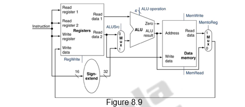
Now, that we have examined the datapath components needed for the individual instruction classes, we can combine them into a single datapath and add the control to complete the implementation. The combined datapath is shown Figure 8.9 below.
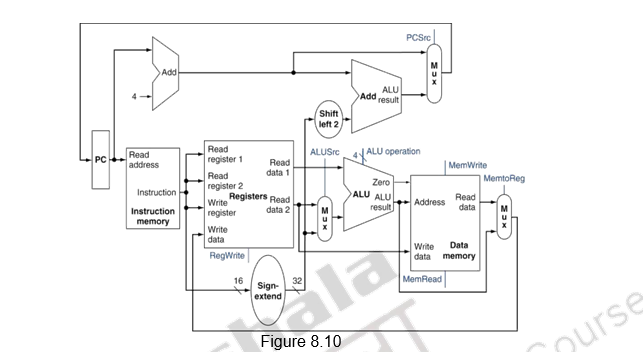
The simplest datapath might attempt to execute all instructions in one clock cycle. This means that no datapath resource can be used more than once per instruction, so any element needed more than once must be duplicated. We therefore need a memory for instructions separate from one for data. Although some of the functional units will need to be duplicated, many of the elements can be shared by different instruction flows. To share a datapath element between two different instruction classes, we may need to allow multiple connections to the input of an element, using a multiplexor and control signal to select among the multiple inputs. While adding multiplexors, we should note that though the operations of arithmetic/logical ( R-type) instructions and the memory related instructions datapath are quite similar, there are certain key differences.
- The R-type instructions use two register operands coming from the register file. The memory instructions also use the ALU to do the address calculation, but the second input is the sign-extended 16-bit offset field from the instruction.
- The value stored into a destination register comes from the ALU for an R-type instruction, whereas, the data comes from memory for a load.
To create a datapath with a common register file and ALU, we must support two different sources for the second ALU input, as well as two different sources for the data stored into the register file. Thus, one multiplexor needs to be placed at the ALU input and another at the data input to the register file, as shown in Figure 8.10.
We have discussed the individual instructions – arithmetic/logical, memory related and branch. Now we can combine all the pieces to make a simple datapath for the MIPS architecture by adding the datapath for instruction fetch, the datapath from R-type and memory instructions and the datapath for branches. Figure below shows the datapath we obtain by combining the separate pieces. The branch instruction uses the main ALU for comparison of the register operands, so we must keep the adder shown earlier for computing the branch target address. An additional multiplexor is required to select either the sequentially following instruction address, PC + 4, or the branch target address to be written into the PC.
To summarize, we have looked at the steps in the execution of a complete instruction with MIPS as a case study. We have incrementally constructed the datapath for the Arithmetic/logical instructions, Load/Store instructions and the Branch instruction. The implementation of the jump instruction to the datapath and the control path implementation will be discussed in the next module.
Web Links / Supporting Materials
- Computer Organization and Design – The Hardware / Software Interface, David A. Patterson and John L. Hennessy, 4th.Edition, Morgan Kaufmann, Elsevier, 2009.
- Computer Organization, Carl Hamacher, Zvonko Vranesic and Safwat Zaky, 5th.Edition, McGraw- Hill Higher Education, 2011.