10 Pipelining – MIPS Implementation
Dr A. P. Shanthi
The objectives of this module are to discuss the basics of pipelining and discuss the implementation of the MIPS pipeline.
In the previous module, we discussed the drawbacks of a single cycle implementation. We observed that the longest delay determines the clock period and it is not feasible to vary period for different instructions. This violates the design principle of making the common case fast. One way of overcoming this problem is to go in for a pipelined implementation. We shall now discuss the basics of pipelining. Pipelining is a particularly effective way of organizing parallel activity in a computer system. The basic idea is very simple. It is frequently encountered in manufacturing plants, where pipelining is commonly known as an assembly line operation. By laying the production process out in an assembly line, products at various stages can be worked on simultaneously. You must have noticed that in an automobile assembly line, you will find that one car’s chassis will be fitted when some other car’s door is getting fixed and some other car’s body is getting painted. All these are independent activities, taking place in parallel. This process is also referred to as pipelining, because, as in a pipeline, new inputs are accepted at one end and previously accepted inputs appear as outputs at the other end. As yet another real world example, Consider the case of doing a laundry. Assume that Ann, Brian, Cathy and Daveeach have one load of clothes to wash, dry, and fold and that the washer takes 30 minutes, dryer takes 40 minutes and the folder takes 20 minutes. Sequential laundry takes 6 hours for 4 loads. On the other hand, if they learned pipelining, how long would the laundry take? It takes only 3.5 hours for 4 loads! For four loads, you get a Speedup = 6/3.5 = 1.7. If you work the washing machine non-stop, you get a Speedup = 110n/40n + 70 ≈ 3 = number of stages.
To apply the concept of instruction execution in pipeline, it is required to break the instruction execution into different tasks. Each task will be executed in different processing elements of the CPU. As we know that there are two distinct phases of instruction execution: one is instruction fetch and the other one is instruction execution. Therefore, the processor executes a program by fetching and executing instructions, one after another. The cycle time τ of an instruction pipeline is the time needed to advance a set of instructions one stage through the pipeline. The cycle time can be determined as
where τm = maximum stage delay (delay through the stage which experiences the largest delay) , k = number of stages in the instruction pipeline, d = the time delay of a latch needed to advance signals and data from one stage to the next. Now suppose that n instructions are processed and these instructions are executed one after another. The total time required Tk to execute all n instructions is
In general, let the instruction execution be divided into five stages as fetch, decode, execute, memory access and write back, denoted by Fi, Di, Ei, Mi and Wi. Execution of a program consists of a sequence of these steps. When the first instruction’s decode happens, the second instruction’s fetch is done. When the pipeline is filled, you see that there are five different activities taking place in parallel. All these activities are overlapped. Five instructions are in progress at any given time. This means that five distinct hardware units are needed. These units must be capable of performing their tasks simultaneously and without interfering with one another. Information is passed from one unit to the next through a storage buffer. As an instruction progresses through the pipeline, all the information needed by the stages downstream must be passed along.
If all stages are balanced, i.e., all take the same time,

If the stages are not balanced, speedup will be less. Observe that the speedup is due to increased throughput and the latency (time for each instruction) does not decrease.
The basic features of pipelining are:
• Pipelining does not help latency of single task, it only helps throughput of entire workload
• Pipeline rate is limited by the slowest pipeline stage
• Multiple tasks operate simultaneously
• It exploits parallelism among instructions in a sequential instruction stream
• Unbalanced lengths of pipe stages reduces speedup
• Time to “fill” pipeline and time to “drain” it reduces speedup
• Ideally the speedup is equal to the number of stages and the CPI is 1
Let us consider the MIPS pipeline with five stages, with one step per stage:
• IF: Instruction fetch from memory
• ID: Instruction decode & register read
• EX: Execute operation or calculate address
• MEM: Access memory operand
• WB: Write result back to register
Consider the details given in Figure 10.1. Assume that it takes 100ps for a register read or write and 200ps for all other stages. Let us calculate the speedup obtained by pipelining.
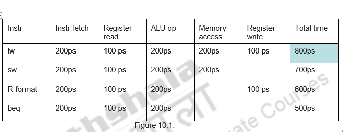
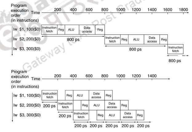
Figure 10.2
For a non pipelined implementation it takes 800ps for each instruction and for a pipelined implementation it takes only 200ps.
Observe that the MIPS ISA is designed in such a way that it is suitable for pipelining.
Figure 10.3 shows the MIPS pipeline implementation.
– All instructions are 32-bits
- Easier to fetch and decode in one cycle
- Comparatively, the x86 ISA: 1- to 17-byte instructions
– Few and regular instruction formats
- Can decode and read registers in one step
– Load/store addressing
- Can calculate address in 3rd stage, access memory in 4th stage
– Alignment of memory operands
- Memory access takes only one cycle
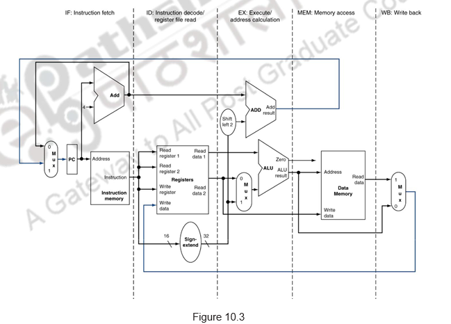
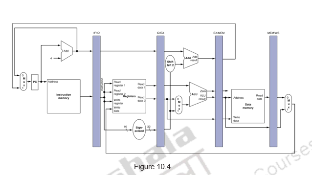
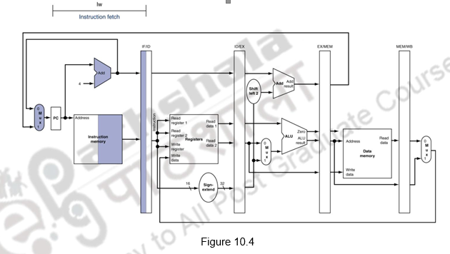
Figure 10.4 shows how buffers are introduced between the stages. This is mandatory. Each stage takes in data from that buffer, processes it and write into the next buffer. Also note that as an instruction moves down the pipeline from one buffer to the next, its relevant information also moves along with it. For example, during clock cycle 4, the information in the buffers is as follows:
- Buffer IF/ID holds instruction I4, which was fetched in cycle 4
- Buffer ID/EX holds the decoded instruction and both the source operands for instruction I3. This is the information produced by the decoding hardware in cycle 3.
- Buffer EX/MEM holds the executed result of I2. The buffer also holds the information needed for the write step of instruction I2. Even though it is not needed by the execution stage, this information must be passed on to the next stage and further down to the Write back stage in the following clock cycle to enable that stage to perform the required Write operation.
- Buffer MEM/WB holds the data fetched from memory (for a load) for I1, and for the arithmetic and logical operations, the results produced by the execution unit and the destination information for instruction I1 are just passed.
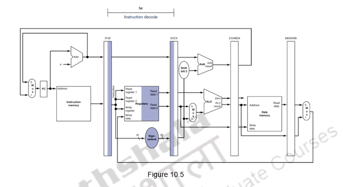
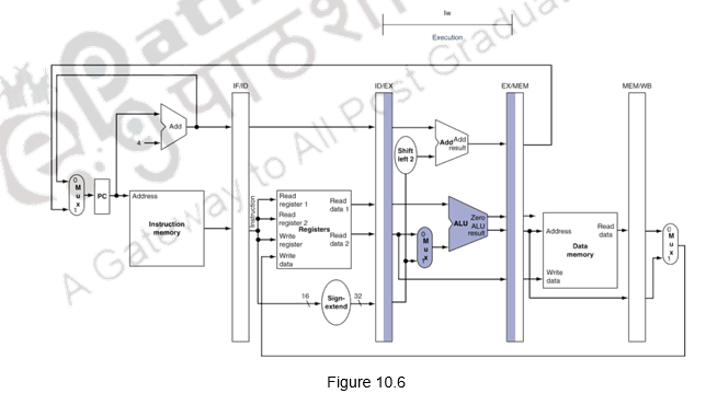
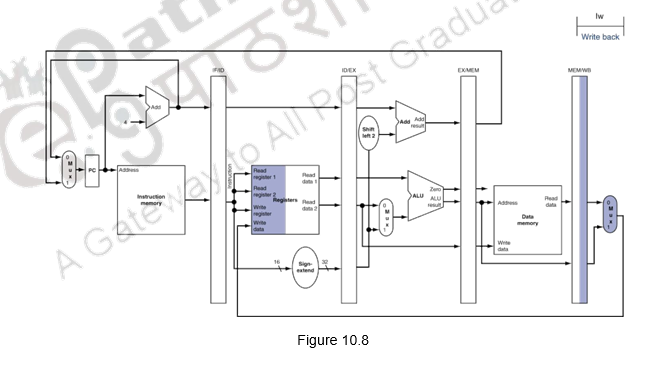
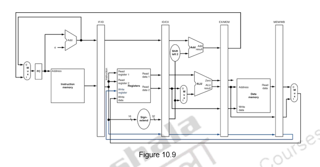
We shall look at the single-clock-cycle diagrams for the load & store instructions of the MIPS ISA. Figure 10.4 shows the instruction fetch for a load / store instruction. Observe that the PC is used to fetch the instruction, it is written into the IF/ID buffer and the PC is incremented by 4. Figure 10.5 shows the next stage of ID. The instruction is decoded, the register file is read and the operands are written into the ID/EX buffer. Note that the entire information of the instruction including the destination register is written into the ID/EX buffer. The highlights in the figure show the resources involved. Figure 10.6 shows the execution stage. The base register’s contents and the sign extended displacement are fed to the ALU, the addition operation is initiated and the ALU calculates the memory address. This effective address is stored in the EX/MEM buffer. Also the destination register’s information is passed from the ID/EX buffer to the EX/MEM buffer. Next, the memory access happens and the read data is written into the MEM/WB buffer. The destination register’s information is passed from the EX/MEM buffer to the MEM/WB buffer. This is illustrated in Figure 10.7. The write back happens in the last stage. The data read from the data memory is written into the destination register specified in the instruction. This is shown in Figure 10.8. The destination register information is passed on from the MEM/WB memory backwards to the register file, along with the data to be written. The datapath is shown in Figure 10.9.
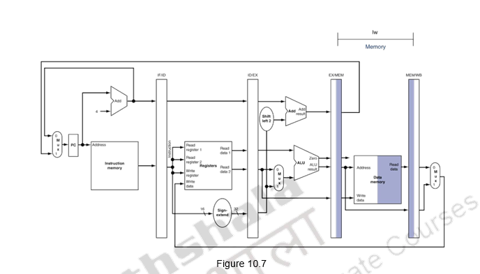
For a store instruction, the effective address calculation is the same as that of load. But when it comes to the memory access stage, store performs a memory write. The effective address is passed on from the execution stage to the memory stage, the data read from the register file is passed from the ID/EX buffer to the EX/MEM buffer and taken from there. The store instruction completes with this memory stage. There is no write back for the store instruction.
While discussing the cycle-by-cycle flow of instructions through the pipelined datapath, we can look at the following options:
- “Single-clock-cycle” pipeline diagram
- Shows pipeline usage in a single cycle
- Highlight resources used
- o “multi-clock-cycle” diagram
- Graph of operation over time
The multi-clock-cycle pipeline diagram showing the resource utilization is given in Figure 10.10. It can be seen that the Instruction memory is used in eth first stage, The register file is used in the second stage, the ALU in the third stage, the data memory in the fourth stage and the register file in the fifth stage again.
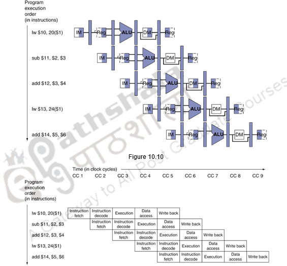
Figure 10.11
The multi-cycle diagram showing the activities happening in each clock cycle is given in Figure 10.11.
Now, having discussed the pipelined implementation of the MIPS architecture, we need to discuss the generation of control signals. The pipelined implementation of MIPS, along with the control signals is given in Figure 10.12.
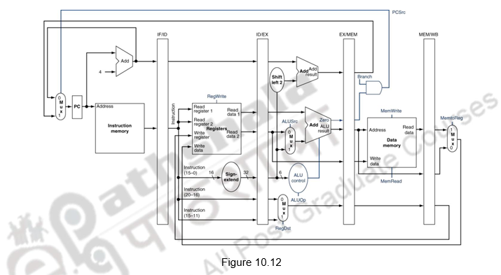
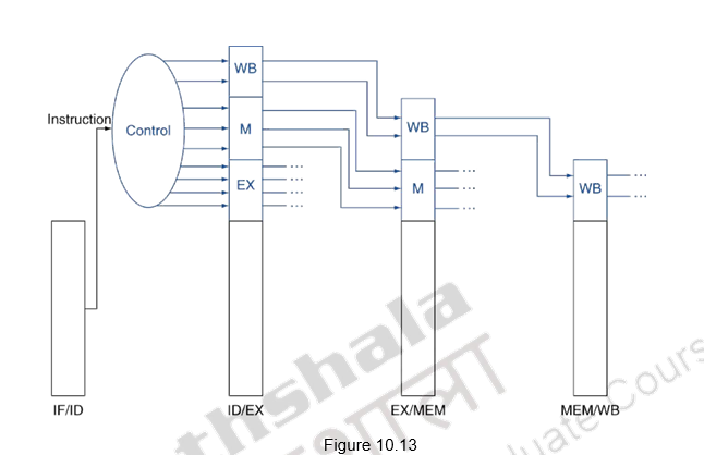
All the control signals indicated are not required at the same time. Different control signals are required at different stages of the pipeline. But the decision about the generation of the various control signals is done at the second stage, when the instruction is decoded. Therefore, just as the data flows from one stage to another as the instruction moves from one stage to another, the control signals also pass on from one buffer to another and are utilized at the appropriate instants. This is shown in Figure 10.13. The control signals for the execution stage are used in that stage. The control signals needed for the memory stage and the write back stage move along with that instruction to the next stage. The memory related control signals are used in the next stage, whereas, the write back related control signals move from there to the next stage and used when the instruction performs the write back operation.
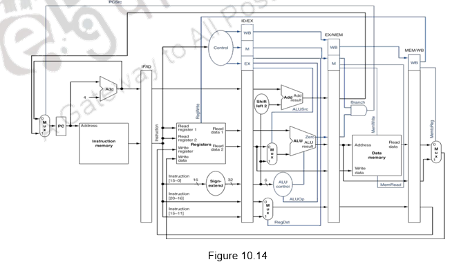
The complete pipeline implementation, along with the control signals used at the various stages is given in Figure 10.14.
To summarize, we have discussed the basics of pipelining in this module. We have made the following observations about pipelining.
- Pipelining is overlapped execution of instructions
- Latency is the same, but throughput improves
- Pipeline rate limited by slowest pipeline stage
- Potential speedup = Number of pipe stages
We have discussed about the implementation of pipelining in the MIPS architecture. We have shown the implementation of the various buffers, the data flow and the control flow for a pipelined implementation of the MIPS architecture.
Web Links / Supporting Materials
- Computer Organization and Design – The Hardware / Software Interface, David A. Patterson and John L. Hennessy, 4th.Edition, Morgan Kaufmann, Elsevier, 2009.
- Computer Organization, Carl Hamacher, Zvonko Vranesic and Safwat Zaky, 5th.Edition, McGraw- Hill Higher Education, 2011.