33 Case Studies of Multicore Architectures I
Dr A. P. Shanthi
The objectives of this module are to discuss about the need for multicore processors and discuss the salient features of the Intel multicore architectures as a case study.
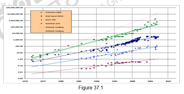
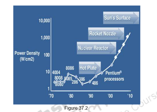
In many of the previous modules, we have looked et different ways of exploiting ILP. ILP is parallelism at the machine -instruction level, through which the processor can re-order, pipeline instructions, use predication, do aggressive branch prediction, etc. ILP had enabled rapid increases in processor speeds for two decades or so. During this period, the transistor densities doubled every 18 months (Moore’s Law) and the frequencies increased making the pipelines deeper and deeper. Figure 37.1 shows the trend that happened. But deeply pipelined circuits had to do deal with the heat generated, due to the rise in temperatures. The design of such complicated processors was difficult and there was also diminishing returns with increasing frequencies. All these made it difficult to make single-core clock frequencies even higher. The power densities increased so rapidly that they had to be somehow contained within limits. Figure 37.2 shows the increase in power densities.
Additionally, from the application point of view also, many new applications are multithreaded. Single-core superscalar processors cannot fully exploit TLP. So, the general trend in computer architecture is to shift towards more parallelism. There has been a paradigm shift from complicated single core architectures to simpler multicore architectures. This is parallelism on a coarser scale – explicitly exploiting TLP.
Multi-core processors take advantage of a fundamental relationship between power and frequency. By incorporating multiple cores, each core is able to run at a lower frequency, dividing among them the power normally given to a single core. The result is a big performance increase over a single-core processor. The following illustration in Figures 37.3 and 37.4 shows this key advantage.
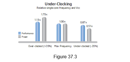
As shown in Figure 37.3, i ncreasing the clock frequency by 20 percent to a single core delivers a 13 percent performance gain, but requires 73 percent greater power. Conversely, decreasing clock frequency by 20 percent reduces power usage by 49 percent, but results in just a 13 percent performance loss.
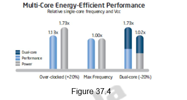
A second core is added to the under-clocked example above. This results in a dual-core processor that at 20 percent reduced clock frequency, effectively delivers 73 percent more performance while using approximately the same power as a single-core processor at maximum frequency. This is shown in Figure 37.4.
A multicore processor is a special kind of a multiprocessor, where all processors are on the same chip. Multicore processors fall under the category of MIMD – different cores execute different threads (Multiple Instructions), operating on different parts of memory (Multiple Data). Multicore is a shared memory multiprocessor, since all cores share the same memory. Therefore, all the issues that we have discussed with MIMD style of shared memory architectures hold good for these processors too.
Multicore architectures can be homogeneous or heterogeneous. Homogeneous processors are those that have identical cores on the chip. Heterogeneous processors have different types of cores on the chip. The software technologists will need to understand the architecture to get appropriate performance gains. With dual core & multicore processors ruling the entire computer industry, some of the architectural issues would be different than the traditional issues . For example, the new performance mantra would be performance per watt.
We shall discuss different multicore architectures as case studies. The following architectures will be discussed:
• Intel
• Sun’s Niagara
• IBM’s Cell BE
Of these, this module will deal with the salient features of the Intel’s multicore architectures.
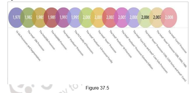
Intel’s Multicore Architectures: Like all other partners in the computer industry, Intel also acknowledged that it had hit a ”thermal wall‘’ in 2004 and disbanded one of its most advanced design groups and said it would abandon two advanced chip development projects. Now, Intel is embarked on a course already adopted by some of its major rivals: obtaining more computing power by stamping multiple processors on a single chip rather than straining to increase the speed of a single processor. The evolution of the Intel processors from 1978 to the introduction of multicore processors is shown in Figure 37.5.
The following are the salient features of the Intel’s multicore architectures:
• Hyper-threading
• Turbo boost technology
• Improved cache latency with smart L3 cache
• New Platform Architecture
• Quick Path Interconnect (QPI)
• Intelligent Power Technology
• Higher Data-Throughput via PCI Express 2.0 and DDR3 Memory Interface
• Improved Virtualization Performance
• Remote Management of Networked Systems with Intel Active Management Technology
• Other improvements – Increase in window size, better branch prediction, more instructions and accelerators, etc.
We shall discuss each one of them in detail.
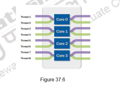
Optimized Multithreaded Performance through Hyper-Threading: Intel introduced Hyper-Threading Technology on its processors in 2002. Hyper -threading exposes a single physical processing core as two logical cores to allow them to share resources between execution threads and therefore increase the system efficiency, as shown in Figure 37.6. Because of the lack of OSs that could clearly differentiate between logical and physical processing cores, Intel removed this feature when it introduced multicore CPUs. With the release of OSs such as Windows Vista and Windows 7, which are fully aware of the differences between logical and physical core, Intel brought back the hyper-threading feature in the Core i7 family of processors. Hyper-threading allows simultaneous execution of two execution threads on the same physical CPU core. With four cores, there are eight threads of execution. Hyper-threading technology benefits from larger caches and increased memory bandwidth of the Core i7 processors, delivering greater throughput and responsiveness for multithreaded applications.
CPU Performance Boost via Intel Turbo Boost Technology: The applications that are run on multicore processors can be single threaded or multi -threaded. In order to provide a performance boost for lightly threaded applications and to also optimize the processor power consumption, Intel introduced a new feature called Intel Turbo Boost. Intel Turbo Boost features offer processing performance gains for all applications regardless of the number of execution threads created. It automatically allows active processor cores to run faster than the base operating frequency when certain conditions are met. This mode is activated when the OS requests the highest processor performance state. The maximum frequency of the specific processing core on the Core i7 processor is dependent on the number of active cores, and the amount of time the processor spends in the Turbo Boost state depends on the workload and operating environment.
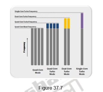
Figure 37.7 illustrates how the operating frequencies of the processing cores in the quad-core Core i7 processor change to offer the best performance for a specific workload type. In an idle state, all four cores operate at their base clock frequency. If an application that creates four discrete execution threads is initiated, then all four processing cores start operating at the quad-core turbo frequency. If the application creates only two execution threads, then two idle cores are put in a low-power state and their power is diverted to the two active cores to allow them to run at an even higher clock frequency. Similar behavior would apply in the case where the applications generate only a single execution thread.
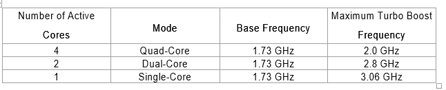
For example, the Intel Core i7-820QM quad-core processor has a base clock frequency of 1.73 GHz. If the application is using only one CPU core, Turbo Boost technology automatically increases the clock frequency of the active CPU core on the Intel Core i7-820QM processor from 1.73 GHz to up to 3.06 GHz and places the other three cores in an idle state, thereby providing optimal performance for all application types. This is shown in the table below.
The duration of time that the processor spends in a specific Turbo Boost state depends on how soon it reaches thermal, power, and current thresholds. With adequate power supply and heat dissipation solutions, a Core i7 processor can be made to operate in the Turbo Boost state for an extended duration of time. In some cases, the users can manually control the number of active processor cores through the controller’s BIOS to fine tune the operation of the Turbo Boost feature for optimizing performance for specific application types.
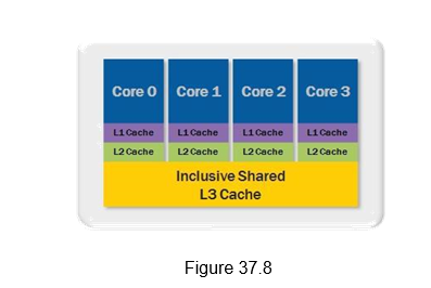
Improved Cache Latency with Smart L3 Cache: All of us are aware of the fact that the cache is a block of high-speed memory for temporary data storage located on the same silicon die as the CPU. If a single processing core, in a multicore CPU, requires specific data while executing an instruction set, it first searches for the data in its local caches (L1 and L2). If the data is not available, also known as a cache-miss, it then accesses the larger L3 cache. In an exclusive L3 cache, if that attempt is unsuccessful, then the core performs cache snooping – searches the local caches of other cores – to check whether they have data that it needs. If this attempt also results in a cache-miss, it then accesses the slower system RAM for that information. The latency of reading and writing from the cache is much lower than that from the system RAM, therefore a smarter and larger cache greatly helps in improving processor performance.
The Core i7 family of processors features an inclusive s hared L3 cache that can be up to 12 MB in size. Figure 37.8 shows the different types of caches and their layout for the Core i7-820QM quad-core processor. It features four cores, where each core has 32 kilobytes for instructions and 32 kilobytes for data of L1 cache, 256 kilobytes per core of L2 cache, along with 8 megabytes of shared L3 cache. The L3 cache is shared across all cores and its inclusive nature helps increase performance and reduces latency by reducing cache snooping traffic to the processor cores. An inclusive shared L3 cache guarantees that if there is a cache-miss, then the data is outside the processor and not available in the local caches of other cores, which eliminates unnecessary cache snooping. This feature provides improvement for the overall performance of the processor and is beneficial for a variety of applications including test, measurement, and control.
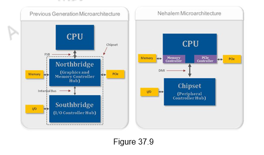
New Platform Architecture: As shown in Figure 37.9, the previous Intel micro-architectures for a single processor system included three discrete components – a CPU, a Graphics and Memory Controller Hub (GMCH), also known as the Northbridge and an I/O Controller Hub (ICH), also known as the Southbridge. The GMCH and ICH combined together are referred to as the chipset. In the older Penryn architecture, the front-side bus (FSB) was the interface for exchanging data between the CPU and the northbridge. If the CPU had to read or write data into system memory or over the PCI Express bus, then the data had to traverse over the external FSB. In the new Nehalem micro-architecture, Intel moved the memory controller and PCI Express controller from the northbridge onto the CPU die, reducing the number of external data buses that the data had to traverse. These changes help increase data-throughput and reduce the latency for memory and PCI Express data transactions. These improvements make the Core i7 family of processors ideal for test and measurement applications such as high-speed design validation and high-speed data record and playback.
Higher – Performance Multiprocessor Systems with Quick Path Interconnect (QPI): Not only was the memory controller moved to the CPU for Nehalem processors, Intel also introduced a distributed shared memory architecture using Intel QuickPath Interconnect (QPI). QPI is the new point-to-point interconnect for connecting a CPU to either a chipset or another CPU. It provides up to 25.6 GB/s of total bidirectional data throughput per link. Intel’s decision to move the memory controller in the CPU and introduce the new QPI data bus has had an impact for single-processor systems. However, this impact is much more significant for multiprocessor systems. Figure 37.10 illustrates the typical block diagrams of multiprocessor systems based on the previous generation and the Nehalem microarchitecture.
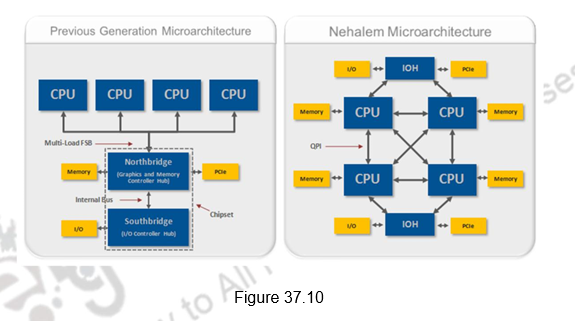
Each CPU has access to local memory but they also can access memory that is local to other CPUs via QPI transactions. For example, one Core i7 processor can access the memory region local to another processor through QPI either with one direct hop or through multiple hops. QPI is a high-speed, point-to-point interconnect. Figure 37.11 illustrates this. It provides high bandwidth and low latency, which delivers the interconnect performance needed to unleash the new microarchitecture and deliver the Reliability, Availability, and Serviceability (RAS) features expected in enterprise applications. RAS requirements are met through advanced features which include: CRC error detection, link-level retry for error recovery, hot-plug support, clock fail-over, and link self-healing. Detection of clock failure & automatic readjustment of the width & clock being transmitted on a predetermined dataline increases availability.
It supports simultaneous movement of data between various components. Support for several features such as lane/polarity reversal, data recovery and deskew circuits, and waveform equalization that ease the design of the high-speed link, are provided. The Intel® QuickPath Interconnect includes a cache coherency protocol to keep the distributed memory and caching structures coherent during system operation. It supports both low-latency source snooping and a scalable home snoop behavior. The coherency protocol provides for direct cache-to-cache transfers for optimal latency.
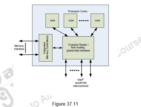
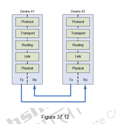
The QPI supports a layered architecture as shown in Figure 37.12. The Physical layer consists of the actual wires, as well as circuitry and logic to support ancillary features required in the transmission and receipt of the 1s and 0s – unit of transfer is 20-bits, called a Phit (for Physical unit). • The Link layer is responsible for reliable transmission and flow control – unit of transfer is an 80-bit Flit (for Flow control unit). The Routing layer provides the framework for directing packets through the fabric. The Transport layer is an architecturally defined layer (not implemented in the initial products) providing advanced routing capability for reliable end-to-end transmission. The Protocol layer is the high-level set of rules for exchanging packets of data between devices. A packet is comprised of an integral number of Flits.
Intelligent Power Technology: Intel’s multicore processors provide intelligent power gates that allow the idling processor cores to near zero power, thus reducing the power consumption. Power consumption is reduced to 10 watts compared to 16 to 50 watts earlier. There is support provided for automated low power states to put the processor and memory in the lowest power state allowable in a workload.
Higher Data-Throughput via PCI Express 2.0 and DDR3 Memory Interface: To support the need of modern applications to move data at a faster rate, the Core i7 processors offer increased throughput for the external databus and its memory channels. The new processors feature the PCI Express 2.0 databus, which doubles the data throughput from PCI Express 1.0 while maintaining full hardware and software compatibility with PCI Express 1.0. A x16 PCI Express 2.0 link has a maximum throughput of 8 GB/s/direction. To allow data from the PCI Express 2.0 databus to be stored in system RAM, the Core i7 processors feature multiple DDR3 1333 MHz memory channels. A system with two channels of DDR3 1333 MHz RAM had a theoretical memory bandwidth of 21.3 GB/s. This throughput matches well with the theoretical maximum throughput of a x16 PCI Express 2.0 link.
Improved Virtualization Performance: Virtualization is a technology that enables running multiple OSs side-by-side on the same processing hardware. In the test, measurement, and control space, engineers and scientists have used this technology to consolidate discrete computing nodes into a single system. With the Nehalem mircoarchitecture, Intel has added new features such as hardware-assisted page-table management and directed I/O in the Core i7 processors and its chipsets that allow software to further improve their performance in virtualized environments.
Remote Management of Networked Systems with Intel Active Management Technology (AMT): AMT provides system administrators the ability to remotely monitor, maintain, and update systems. Intel AMT is part of the Intel Management Engine, which is built into the chipset of a Nehalem-based system. This feature allows administrators to boot systems from a remote media, track hardware and software assets, and perform remote troubleshooting and recovery. Engineers can use this feature for managing deployed automated test or control systems that need high uptime. Test, measurement, and control applications are able to use AMT to perform remote data collection and monitor application status. When an application or system failure occurs, AMT enables the user to remotely diagnose the problem and access debug screens. This allows for the problem to be resolved sooner and no longer requires interaction with the actual system. When software updates are required, AMT allows for these to be done remotely, ensuring that the system is updated as quickly as possible since downtime can be very costly. AMT is able to provide many remote management benefits for PXI systems.
Other Improvements: Apart from the features discussed above, there are also other improvements brought in. They are listed below:
• Greater Parallelism
- Increase amount of code that can be executed out-of-order by increasing the size of the window and scheduler
• Efficient algorithms
- Improved performance of synchronization primitives
- Faster handling of branch mis-prediction
- Improved hardware prefetch & better Load-Store scheduling
• Enhanced Branch Prediction
- New Second-Level Branch Target Buffer(BTB)
- New Renamed Return Stack Buffer (RSB)
• New Application Targeted Accelerators and Intel SSE4 (Streaming SIMD extensions-4)
- Enable XML parsing/accelerators
To summarize, we have dealt in detail the salient features of intel’s multicore architectures in this module. The following features were discussed:
- Hyper-threading
- Turbo boost technology
- Improved cache latency with smart L3 cache
- New Platform Architecture
- Quick Path Interconnect (QPI)
- Intelligent Power Technology
- Higher Data-Throughput via PCI Express 2.0 and DDR3 Memory Interface
- Improved Virtualization Performance
- Remote Management of Networked Systems with Intel Active Management Technology
- Other improvements
Web Links / Supporting Materials
- Computer Architecture – A Quantitative Approach , John L. Hennessy and David A. Patterson, 5th Edition, Morgan Kaufmann, Elsevier, 2011.
- Intel White Papers:
- https://www.pogolinux.com/learn/files/quad-core-06.pdf
- Intel Tech/Research: http://www.intel.com/technology/index.htm
- Energy Efficient Performance: http://www.intel.com/technology/eep/index.htm
- Intel Core Microarchitecture: http://www.intel.com/technology/architecture/coremicro/
- Dual-core processor: http://www.intel.com/technology/computing/dual-core/index.htm
- Multi/Many Core: http://www.intel.com/multi-core/index.htm
- Intel Platforms: http://www.intel.com/platforms/index.htm
- Threading: http://www3.intel.com/cd/ids/developer/asmo-na/eng/dc/threading/index.htm
- Top Eight Features of the Intel Core i7 Processors for Test, Measurement, and Control:
- http://www.ni.com/white-paper/11266/en/#toc1