21 Memory Hierarchy Design – Basics
Dr A. P. Shanthi
The objectives of this module are to discuss about the need for a hierarchical memory system and also discuss about the different types of memories that are available.
The previous modules dealt with the Central Processing Unit (CPU), where we discussed about the Arithmetic and Logical Unit (ALU) and the control path implementation. We also looked at different techniques for improving the performance of processors by exploiting ILP. This module discusses about another component of the digital computer – viz., memory.
Whenever we look at the memory system, we would want to have fast, large and also cheap memories. Now, having all that together is not possible. Faster memories are more expensive and may also occupy more space. Therefore, having all these features together in a memory system is not practical and the only solution to reap all the benefits is to have a hierarchical memory system.
In a hierarchical memory system, the entire addressable memory space is available in the largest, slowest memory and incrementally smaller and faster memories, each containing a subset of the memory below it, proceed in steps up toward the processor. This hierarchical organization of memory works primarily because of the Principle of Locality. That is, the program accesses a relatively small portion of the address space at any instant of time. We are aware of the statement that the processor spends 90% of the time on 10% of the code. There are basically two different types of locality: temporal and spatial.
- Temporal Locality (Locality in Time): If an item is referenced, it will tend to be referenced again soon (e.g., loops, reuse)
- Spatial Locality (Locality in Space): If an item is referenced, items whose addresses are close by tend to be referenced soon (e.g., straightline code, array access) And for the past two decades or so, the hardware has relied on the principle of locality for providing speed.
Temporal and spatial locality insure that nearly all references can be found in smaller memories and at the same time gives the illusion of a large, fast memory being presented to the processor. Figure 25.1 shows a hierarchical memory system. The faster, smaller and more expensive memories are closer to the processor. As we move away from the processor, the speed decreases, cost decreases and the size increases. The registers and cache memories are closer to the processor, satisfying the speed requirements of the processor, the main memory comes next and last of all, the secondary storage which satisfies the capacity requirements. Indicated in the figure are also the typical sizes and access times of each of these types of memories. The registers which are part of the CPU itself have very low access times of a few hundreds of picoseconds and the storage space is a few thousand of bytes. The first level cache has a few kilobytes and the access times are only a few nanoseconds. The second level cache has a few hundred kilobytes and the access times increase to about 10 nanoseconds. The storage increases to a few megabytes in the case of the third level of cache, and the access times increase to a few tens of nanoseconds. The main memory has access times in the order of a few hundreds of nanoseconds, but also has larger storage. Storage is in order of terabytes for the secondary storage and the access times go to a few milliseconds. Following along the same lines, the figure also shows the memory hierarchy for a personal mobile device.
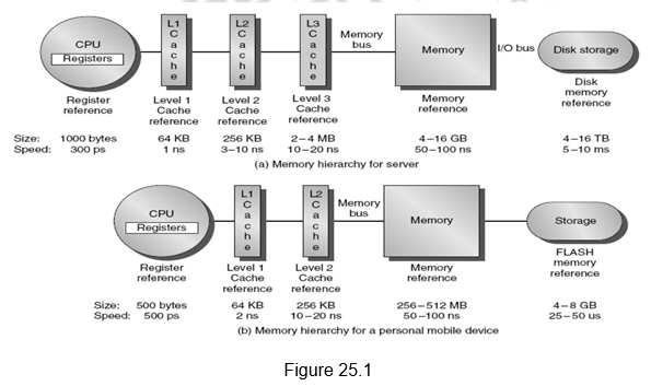
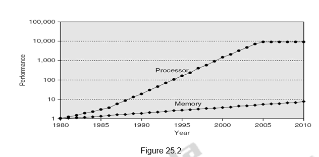
Figure 25.2 shows the memory performance gap. Although people have come up with different technological advancements to increase the speed of the processors as well as memory, the memory speeds have not kept up with the processor speeds, as indicated in Figure 25.2. The hierarchical memory system tries to hide the disparity in speed by placing the fastest memories near the processor.
Memory hierarchy design becomes more crucial with recent multi-core processors because the aggregate peak bandwidth grows with the number of cores. For example, Intel Core i7 can generate two references per core per clock. With four cores and 3.2 GHz clock, there are 25.6 billion 64-bit data references/second and 12.8 billion 128-bit instruction references= 409.6 GB/s. The DRAM bandwidth is only 6% of this (25 GB/s). Therefore, apart from a hierarchical memory system, we require different optimizations like Multi-port, pipelined caches, two levels of cache per core and shared third-level cache on chip. High-end microprocessors typically have more than 10 MB on-chip cache and it is to be noted that this consumes large amount of area and power budget.
Different types of memory: There are different types of memory available. One classification is based on the access types. A Random Access Memory (RAM) has the same access time for all locations. There are two types of RAM – Dynamic and Static RAM. Dynamic Random Access Memory has high density, consumes less power, is cheap and slow. It is called dynamic, because it needs to be “refreshed” regularly. An SRAM – Static Random Access Memory has low density, consumes high power, is expensive and fast. Here, the content will last “forever” (until power is lost). We also have “Not-so-random” Access Technology, where the access time varies from location to location and from time to time. Examples for this type of memory include disks and CDROMs. There is also one more type of memory, viz., sequential access memory where the access time is linear in location (e.g.,Tape). Normally, Dynamic RAM (DRAM) is used for main memory and Static RAM (SRAM) is used for cache.
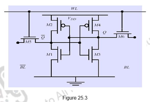
Static RAM: Figure 25.3 gives the construction of a typical SRAM cell. It requires six transistors for construction – hence the reduced density and increased cost. The six transistors are connected in a cross connected fashion. They provide regular and inverted outputs. Since it is implemented using CMOS process, it requires low power to retain the bit.
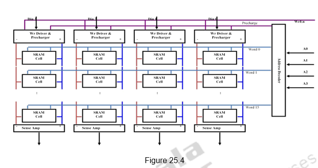
Organization of SRAM Memory: Figure 25.4 shows the single dimensional organization of an SRAM memory consisting of 16 words of 4-bits each. The four address bits are given to the address decoder which selects one of the 16 words. All bits of that word are selected. Write Enable signal is used to enable the write operation. The Data input lines are used to write fresh data into the selected word and the Data output lines are used to read data from the selected word.
Dynamic RAM: A DRAM cell is made up of a single transistor and a capacitor, as shown in Figure 25.5, leading to reduced cost and storage space. However, this is a destructive read out. It needs to be periodically refreshed, say every 8 ms., but each row can be refreshed simultaneously. For a write operation, we have to drive the bit line and select the row. For a read operation, we have to precharge the bit line to Vdd and select the row. The cell and bit line share charges and there is very small voltage change on the bit line. The sense amplifier can detect changes of ~1 million electrons. Once the read is performed, a write is to be done to restore the value. Refresh is just a dummy read to every cell. The advantage of DRAM is its structural simplicity: only one transistor and a capacitor are required per bit, compared to four or six transistors in SRAM. This allows DRAM to reach very high densities. The transistors and capacitors used are extremely small; billions can fit on a single memory chip. Due to the dynamic nature of its memory cells, DRAM consumes relatively large amounts of power, with different ways for managing the power consumption.
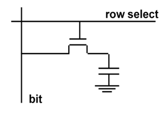
Figure 25.5
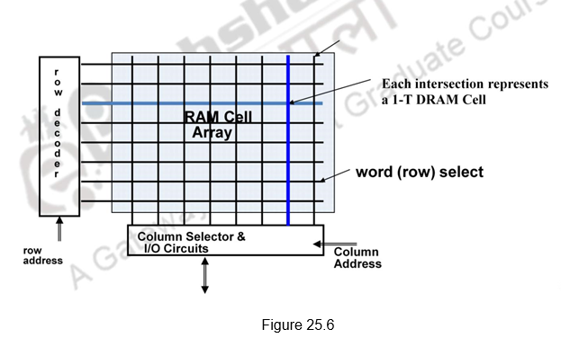
Organization of DRAM Memory: Figure 25.6 shows the two dimensional organization of DRAM. The cells are arranged as a two dimensional array. The address lines are divided into two parts – one part used for the row decoder and the other part for the column decoder. Only the cell that is selected by the row and column decoder can be read or written. As always, though the Data input and Data output lines are not shown, they are used for the Write and Read operations, respectively. In order to conserve the number of address lines, the address lines can be multiplexed. The upper half of address can be transmitted first and then the lower half of the address. The Row Address Strobe (RAS) indicates that the row address is transmitted and the Column Address Strobe (CAS) indicates that the column address is being transmitted.
Memory Optimizations: We know that even though faster memory technologies have been brought in, the speed of memory is still not comparable to the processor speeds. This is a major bottleneck. Recall Amdahl’s law which specifies that there will be a limitation on the overall performance if the common operations like memory operations are not speeded up. Memory capacity and speed should grow linearly with processor speed. However, unfortunately, memory capacity and speed has not kept pace with processors. Therefore, we can think of some optimizations to improve memory accesses. The optimizations that are normally carried out are:
- Multiple accesses to same row
- Synchronous DRAM
- Added clock to DRAM interface
- Burst mode with critical word first
- Wider interfaces
- Double data rate (DDR)
- Multiple banks on each DRAM device
Different types of DRAM: Based on the optimizations performed, there are different types of DRAMS.
Synchronous DRAM, SDRAM, is designed to synchronize itself with the timing of the CPU. This enables the memory controller to know the exact clock cycle when the requested data will be ready. Therefore, the CPU no longer has to wait between memory accesses. SDRAM chips also take advantage of interleaving and burst mode functions, which make memory retrieval even faster. SDRAM modules come in several different speeds so as to synchronize itself with the CPU’s bus they’ll be used in. The maximum speed that SDRAM will run is limited by the bus speed of the computer. SDRAM is the most common type of DRAM found in today’s personal computers. Power consumed can be reduced in SDRAMs by lowering the voltage and using the low power mode which ignores the clock and continues to refresh.
Double Data Rate SDRAM (DDR SDRAM) is a new type of SDRAM technology that supports data transfers on both edges of each clock cycle (the rising and falling edges), effectively doubling the memory chip’s data throughput. For example, with DDR SDRAM, a 100 or 133MHz memory bus clock rate yields an effective data rate of 200MHz or 266MHz. DDR SDRAM uses additional power and ground lines and requires 184-pin DIMM modules rather than the 168-pin DIMMs used by SDRAM. DDR SDRAM also consumes less power, which makes it well suited to notebook computers.
Direct Rambus DRAM (RDRAM) is a new DRAM architecture and interface standard that challenges traditional main memory designs. It transfers data at speeds up to 800MHz over a narrow 16-bit bus called a Direct Rambus Channel. This high-speed clock rate is possible due to a feature called “double clocked,” which allows operations to occur on both the rising and falling edges of the clock cycle. Rambus is designed to fit into existing motherboard standards. The components that are inserted into motherboard connections are called Rambus in-line memory modules (RIMMs). They replace conventional DIMMs. DDR SDRAM and RDRAM compete in the high performance end of the microcomputer market. Because of its new architecture a RDRAM system is somewhat more expensive than DDR SDRAM. Many computer companies make high-end microcomputers with both memory systems and let the consumer make their choice.
Graphics double data rate SDRAM (GDDR SDRAM) is a type of specialized DDR SDRAM designed to be used as the main memory of graphics processing units (GPUs). GDDR SDRAM is distinct from commodity types of DDR SDRAM such as DDR3, although they share some core technologies. Their primary characteristics are higher clock frequencies for both the DRAM core and I/O interface, which provides greater memory bandwidth for GPUs. As of 2015, there are four successive generations of GDDR: GDDR2, GDDR3, GDDR4, and GDDR5.
Read Only Memory (ROM) is a type of non-volatile memory used in computers and other electronic devices. Data stored in ROM can only be modified slowly, with difficulty, or not at all, so it is mainly used to store firmware, as BIOS of desktop computers and in embedded devices (also serves as a code protection device). We have ROMs that are read-only in normal operation, but can still be reprogrammed in some way. Erasable programmable read-only memory (EPROM) and electrically erasable programmable read-only memory (EEPROM) can be erased and re-programmed, but usually this can only be done at relatively slow speeds, may require special equipment to achieve, and is typically only possible a certain number of times.
Flash memory is an electronic non-volatile computer storage medium that can be electrically erased and reprogrammed. It is a type of EEPROM. It must be erased (in blocks) before being overwritten. It has limited number of write cycles. It is cheaper than SDRAM, but more expensive than disk. It is slower than SRAM, and faster than disk. It is extensively used in PDAs, digital audio players, digital cameras, mobile phones, etc. Its mechanical shock resistance is the reason for its popularity over hard disks in portable devices, as also its high durability, being able to withstand high pressure, temperature, immersion in water, etc.
Memory hierarchy terminology: Let us now look at the terminology that is used with a hierarchical memory system. A Hit is said to occur if data appears in some block in the upper level. Hit Rate is the fraction of memory access found in the upper level and Hit Time is the time to access the upper level which consists of RAM access time + Time to determine hit/miss. A Miss is said to occur if data needs to be retrieved from a block in the lower level. Miss Rate = 1 – (Hit Rate). Miss Penalty is the time to replace a block in the upper level + Time to deliver the block to the processor. Hit Time is normally << Miss Penalty. When a word is not found in the cache, a miss occurs:
• Fetch word from lower level in hierarchy, requiring a higher latency reference
• Lower level may be another cache or the main memory
• Also fetch the other words contained within the block
• Takes advantage of spatial locality
Performance Metrics: Latency is a concern of cache and bandwidth is a concern of multiprocessors and I/O. The access time is the time between read request and when desired word arrives. The Cycle time is the minimum time between unrelated requests to memory.
Example to show the impact on performance: Suppose a processor executes at a Clock Rate = 200 MHz (5 ns per cycle) with a CPI = 1.1 and with 50% arithmetic/logical, 30% load/store, 20% control instructions. Suppose that 10% of memory operations get 50 cycle miss penalty.
| Ideal CPI | 1.1 |
| Data Miss | 1.5 |
| Inst Miss | 0.5 |
CPI = ideal CPI + average stalls per instruction= 1.1(cycles) + ( 0.30 (datamops/ins) x 0.10 (miss/datamop) x 50 (cycle/miss) )
= 1.1 cycle + 1.5 cycle = 2. 6
This shows that 58 % of the time the processor is stalled waiting for memory! Adding a a 1% instruction miss rate would add an additional 0.5 cycles to the CPI.
This shows us how important the memory hierarchy design is. The data transfer between registers and memory is managed by the compiler and programmer. The data transfer between cache and memory is managed by the hardware. And the transfer between the memory and disks is managed by the hardware and operating system (virtual memory) and by the programmer (files).
To summarize, a hierarchical memory system is needed to meet the speed, capacity and cost requirements. There are two different types of locality exploited:
– Temporal Locality (Locality in Time): If an item is referenced, it will tend to be referenced again soon
– Spatial Locality (Locality in Space): If an item is referenced, items whose addresses are close by tend to be referenced soon
By taking advantage of the principle of locality, we present the user with as much memory as is available in the cheapest technology and provide access at the speed offered by the fastest technology. SRAMs and DRAMs are very useful as cache and main memory, respectively. Other types of memories like ROM and Flash memories are also very useful. DRAM is slow but cheap and dense. It is a good choice for presenting the user with a BIG memory system. SRAM is fast but expensive and not very dense and is a good choice for providing the user FAST access time.
Web Links / Supporting Materials
- Computer Organization and Design – The Hardware / Software Interface, David A. Patterson and John L. Hennessy, 4th Edition, Morgan Kaufmann, Elsevier, 2009.
- Computer Architecture – A Quantitative Approach , John L. Hennessy and David A.Patterson, 5th Edition, Morgan Kaufmann, Elsevier, 2011.
- Computer Organization, Carl Hamacher, Zvonko Vranesic and Safwat Zaky, 5th.Edition, McGraw- Hill Higher Education, 2011.