9 Execution of a Complete Instruction – Control Flow
Dr A. P. Shanthi
Execution of a Complete Instruction – Control Flow
The objectives of this module are to discuss how the control flow is implemented when an instruction gets executed in a processor, using the MIPS architecture as a case study and discuss the basics of microprogrammed control.
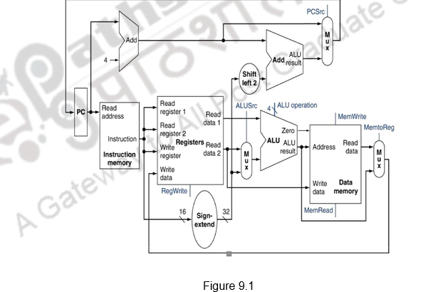
The control unit must be capable of taking inputs about the instruction and generate all the control signals necessary for executing that instruction, for eg. the write signal for each state element, the selector control signal for each multiplexor, the ALU control signals, etc. Figure 9.1 below shows the complete data path implementation for the MIPS architecture along with an indication of the various control signals required.
We shall first of all look at the ALU control. The implementation discussed here is specifically for the MIPS architecture and for the subset of instructions pointed out earlier. You just need to get the concepts from this discussion. The ALU uses 4 bits for control. Out of the 16 possible combinations, only 6 are used for the subset under consideration. This is indicated in Figure 9.2. Depending on the type of instruction class, the ALU will need to perform one of the first five functions. (NOR is needed for other parts of the MIPS instruction set not discussed here.) For the load word and store word instructions, we use the ALU to compute the memory address. This is done by addition. For the R-type instructions, the ALU needs to perform one of the five actions (AND, OR, subtract, add, or set on less than), depending on the value of the 6-bit funct (or function) field in the low-order bits of the instruction (refer to the instruction formats). For a branch on equal instruction, the ALU must perform a subtraction, for comparison.
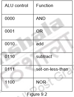
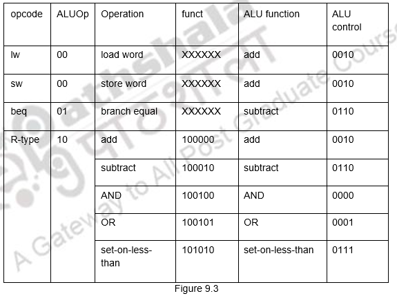
We can generate the 4-bit ALU control input using a small control unit that takes as inputs the function field of the instruction and a 2-bit control field, which we call ALUOp. ALUOp indicates whether the operation to be performed should be add (00) for loads and stores, subtract (01) for beq, or determined by the operation encoded in the funct field (10). The output of the ALU control unit is a 4-bit signal that directly controls the ALU by generating one of the 4-bit combinations shown previously. In Figure 9.3, we show how to set the ALU control inputs based on the 2-bit ALUOp control and the 6-bit function code. The opcode, listed in the first column, determines the setting of the ALUOp bits. When the ALUOp code is 00 or 01, the desired ALU action does not depend on the function code field and this is indicated as don’t cares, and the funct field is shown as XXXXXX. When the ALUOp value is 10, then the function code is used to set the ALU control input.
For completeness, the relationship between the ALUOp bits and the instruction opcode is also shown. Later on we will see how the ALUOp bits are generated from the main control unit. This style of using multiple levels of decoding—that is, the main control unit generates the ALUOp bits, which then are used as input to the ALU control that generates the actual signals to control the ALU unit—is a common implementation technique. Using multiple levels of control can reduce the size of the main control unit. Using several smaller control units may also potentially increase the speed of the control unit. Such optimizations are important, since the control unit is often performance-critical.
There are several different ways to implement the mapping from the 2-bit ALUOp field and the 6-bit funct field to the three ALU operation control bits. Because only a small number of the 64 possible values of the function field are of interest and the function field is used only when the ALUOp bits equal 10, we can use a small piece of logic that recognizes the subset of possible values and causes the correct setting of the ALU control bits.
Now, we shall consider the design of the main control unit. For this, we need to remember the following details about the instruction formats of the MIPS ISA. All these details are indicated in Figure 9.4.
- For all the formats, the opcode field is always contained in bits 31:26 – Op[5:0]
- The two registers to be read are always specified by the Rs and Rt fields, at positions 25:21 and 20:16. This is true for the R-type instructions, branch on equal, and for store
- The base register for the load and store instructions is always in bit positions 25:21 (Rs)
- The destination register is in one of two places. For a load it is in bit positions 20:16 (Rt), while for an R-type instruction it is in bit positions 15:11 (Rd). To select one of these two registers, a multiplexor is needed.
- The 16-bit offset for branch equal, load, and store is always in positions 15:0.
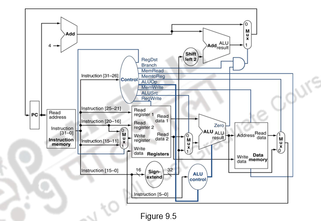
To the simple datapath already shown, we shall add all the required control signals. Figure 9.5 shows these additions plus the ALU control block, the write signals for state elements, the read signal for the data memory, and the control signals for the multiplexors. Since all the multiplexors have two inputs, they each require a single control line. There are seven single-bit control lines plus the 2-bit ALUOp control signal. The seven control signals are listed below:
1. RegDst: The control signal to decide the destination register for the register write operation – The register in the Rt field or Rd field
2. RegWrite: The control signal for writing into the register file
3. ALUSrc: The control signal to decide the ALU source – Register operand or sign extended operand
4. PCSrc: The control signal that decides whether PC+4 or the target address is to written into the PC
5. MemWrite: The control signal which enables a write into the data memory
6. MemRead: The control signal which enables a read from the data memory
7. MemtoReg: The control signal which decides what is written into the register file, the result of the ALU operation or the data memory contents.
The datapath along with the control signals included is shown in Figure 9.5. Note that the control unit takes in the opcode information from the fetched instruction and generates all the control signals, depending on the operation to be performed.
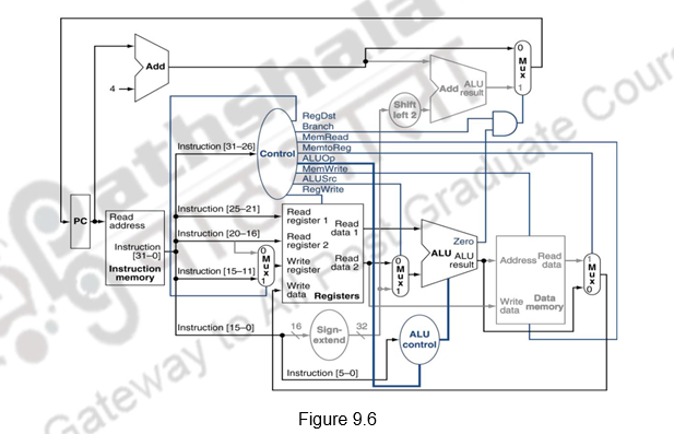
Now, we shall trace the execution flow for different types of instructions and see what control signals have to be activated. Let us consider the execution of an R type instruction first. For all these instructions, the source register fields are Rs and Rt, and the destination register field is Rd. The various operations that take place for an arithmetic / logical operation with register operands are:
- The instruction is fetched from the code memory
- Since the Branch control signal is set to 0, the PC is unconditionally replaced with PC + 4
- The two registers specified in the instruction are read from the register file
- The ALU operates on the data read from the register file, using the function code (bits 5:0, which is the funct field, of the instruction) to generate the ALU function
- The ALUSrc control signal is deasserted, indicating that the second operand comes from a register
- The ALUOp field for R-type instructions is set to 10 to indicate that the ALU control should be generated from the funct field
- The result from the ALU is written into the register file using bits 15:11 of the instruction to select the destination register
- The RegWrite control signal is asserted and the RegDst control signal is made 1, indicating that Rd is the destination register
- The MemtoReg control signal is made 0, indicating that the value fed to the register write data input comes from the ALU
Furthermore, an R-type instruction writes a register (RegWrite = 1), but neither reads nor writes data memory. So, the MemRead and MemWrite control signals are set to 0. These operations along with the required control signals are indicated in Figure 9.6.
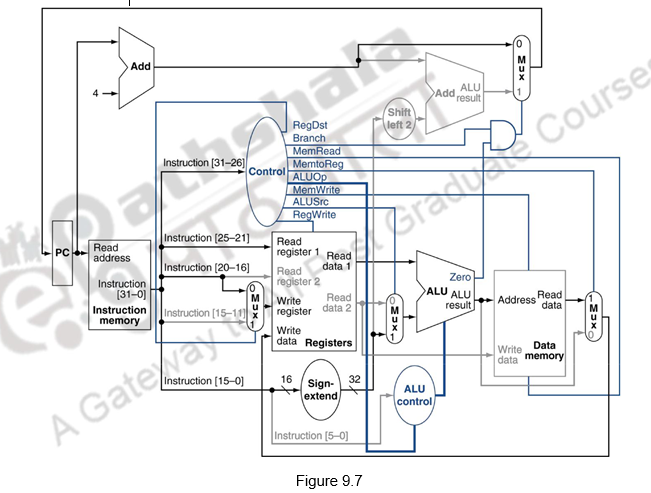
Similarly, we can illustrate the execution of a load word, such as lw $t1, offset($t2). Figure 9.7 shows the active functional units and asserted control lines for a load. We can think of a load instruction as operating in five steps:
- The instruction is fetched from the code memory
- Since the Branch control signal is set to 0, the PC is unconditionally replaced with PC + 4
- A register ($t2) value is read from the register file
- The ALU computes the sum of the value read from the register file and the sign-extended, lower 16 bits of the instruction (offset)
- The ALUSrc control signal is asserted, indicating that the second operand comes from the sign extended operand
- The ALUOp field for R-type instructions is set to 00 to indicate that the ALU should perform addition for the address calculation
- The sum from the ALU is used as the address for the data memory and a data memory read is performed
- The MemRead is asserted and the MemWrite control signals is set to 0
- The result from the ALU is written into the register file using bits 20:16 of the instruction to select the destination register
- The RegWrite control signal is asserted and the RegDst control signal is made 0, indicating that Rt is the destination register
- The MemtoReg control signal is made 1, indicating that the value fed to the register write data input comes from the data memory
A store instruction is similar to the load for the address calculation. It finishes in four steps The control signals that are different from load are:
- MemWrite is 1 and MemRead is 0
- RegWrite is 0
- MemtoReg and RegDst are X’s (don’t cares)
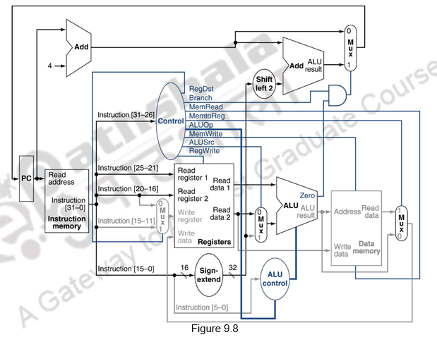
The branch instruction is similar to an R-format operation, since it sends the Rs and Rt registers to the ALU. The ALUOp field for branch is set for a subtract (ALU control = 01), which is used to test for equality. The MemtoReg field is irrelevant when the RegWrite signal is 0. Since the register is not being written, the value of the data on the register data write port is not used. The Branch control signal is set to 1. The ALU performs a subtract on the data values read from the register file. The value of PC + 4 is added to the sign-extended, lower 16 bits of the instruction (offset) shifted left by two; the result is the branch target address. The Zero result from the ALU is used to decide which adder result to store into the PC. The control signals and the data flow for the Branch instruction is shown in Figure 9.8.
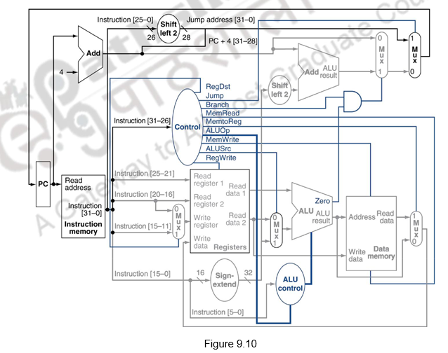
Now, to the subset of instructions already discussed, we shall add a jump instruction. The jump instruction looks somewhat similar to a branch instruction but computes the target PC differently and is not conditional. Like a branch, the low order 2 bits of a jump address are always 00. The next lower 26 bits of this 32-bit address come from the 26-bit immediate field in the instruction, as shown in Figure 9.9. The upper 4 bits of the address that should replace the PC come from the PC of the jump instruction plus 4. Thus, we can implement a jump by storing into the PC the concatenation of the upper 4 bits of the current PC + 4 (these are bits 31:28 of the sequentially following instruction address), the 26-bit immediate field of the jump instruction and the bits 00.
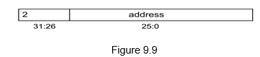
Figure 9.10 shows the addition of the control for jump added to the previously discussed control.
An additional multiplexor is used to select the source for the new PC value, which is either the incremented PC (PC + 4), the branch target PC, or the jump target PC. One additional control signal is needed for the additional multiplexor. This control signal, called Jump, is asserted only when the instruction is a jump—that is, when the opcode is 2.
Since we have assumed that all the instructions get executed in one clock cycle, the longest instruction determines the clock period. For the subset of instructions considered, the critical path is that of the load, which takes the following path Instruction memory ® register file ® ALU ® data memory ® register file
The single cycle implementation may be acceptable for this simple instruction set, but it is not feasible to vary the period for different instructions, for eg. Floating point operations. Also, since the clock cycle is equal to the worst case delay, there is no point in improving the common case, which violates the design principle of making the common case fast. In addition, in this single-cycle implementation, each functional unit can be used only once per clock. Therefore, some functional units must be duplicated, raising the cost of the implementation. A single-cycle design is inefficient both in its performance and in its hardware cost. These shortcomings can be avoided by using implementation techniques that have a shorter clock cycle—derived from the basic functional unit delays—and that require multiple clock cycles for each instruction. In the next module, we will look at another implementation technique, called pipelining, that uses a datapath very similar to the single-cycle datapath, but is much more efficient.
Next, we shall briefly discuss another type of control, viz. microprogrammed control. In the case of hardwired control, we saw how all the control signals required inside the CPU can be generated using hardware. There is an alternative approach by which the control signals required inside the CPU can be generated. This alternative approach is known as microprogrammed control unit. In microprogrammed control unit, the logic of the control unit is specified by a microprogram. A microprogram consists of a sequence of instructions in a microprogramming language. These are instructions that specify microoperations. A microprogrammed control unit is a relatively simple logic circuit that is capable of (1) sequencing through microinstructions and (2) generating control signals to execute each microinstruction.
The concept of microprogram is similar to computer program. In computer program the complete instructions of the program is stored in main memory and during execution it fetches the instructions from main memory one after another. The sequence of instruction fetch is controlled by the program counter (PC). Microprograms are stored in microprogram memory and the execution is controlled by the microprogram counter ( PC). Microprograms consist of microinstructions which are nothing but strings of 0’s and 1’s. In a particular instance, we read the contents of one location of microprogram memory, which is nothing but a microinstruction. Each output line (data line) of microprogram memory corresponds to one control signal. If the contents of the memory cell is 0, it indicates that the signal is not generated and if the contents of memory cell is 1, it indicates the generation of the control signal at that instant of time.
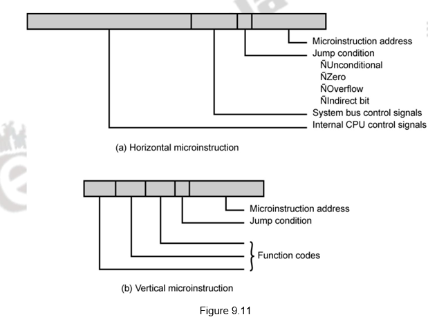
There are basically two types of microprogrammed control – horizontal organization and vertical organization. In the case of horizontal organization, as mentioned above, you can assume that every bit in the control word corresponds to a control signal. In the case of a vertical organization, the signals are grouped and encoded in order to reduce the size of the control word. Normally some minimal level of encoding will be done even in the case of horizontal control. The fields will remain encoded in the control memory and they must be decoded to get the individual control signals. Horizontal organization has more control over the potential parallelism of operations in the datapath; however, it uses up lots of control store. Vertical organization, on the other hand, is easier to program, not very different from programming a RISC machine in assembly language, but needs extra level of decoding and may slow the machine down. Figure 9.11 shows the two formats.
The different terminologies related to microprogrammed control unit are:
Control Word (CW) : Control word is defined as a word whose individual bits represent the various control signal. Therefore each of the control steps in the control sequence of an instruction defines a unique combination of 0s and 1s in the CW. A sequence of control words (CWs) corresponding to the control sequence of a machine instruction constitute the microprogram for that instruction. The individual control words in this microprogram are referred to as microinstructions. The microprograms corresponding to the instruction set of a computer are stored in a special memory that will be referred to as the microprogram memory or control store. The control words related to all instructions are stored in the microprogram memory.
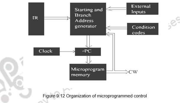
The control unit can generate the control signals for any instruction by sequencially reading the CWs of the corresponding microprogram from the microprogram memory. To read the control word sequentially from the microprogram memory a microprogram counter ( PC) is needed. The basic organization of a microprogrammed control unit is shown in the Figure 3.7. The starting address generator block is responsible for loading the starting address of the microprogram into the PC everytime a new instruction is loaded in the IR. The PC is then automatically incremented by the clock, and it reads the successive microinstruction from memory. Each microinstruction basically provides the required control signal at that time step. The microprogram counter ensures that the control signal will be delivered to the various parts of the CPU in correct sequence.
We have some instructions whose execution depends on the status of condition codes and status flag, as for example, the branch instruction. During branch instruction execution, it is required to take the decision between alternative actions. To handle such type of instructions with microprogrammed control, the design of the control unit is based on the concept of conditional branching in the microprogram. In order to do that, it is required to include some conditional branch microinstructions. In conditional microinstructions, it is required to specify the address of the microprogram memory to which the control must be directed to. It is known as the branch address. Apart from the branch address, these microinstructions can specify which of the states flags, condition codes, or possibly, bits of the instruction register should be checked as a condition for branching to take place.
In a computer program we have seen that execution of every instruction consists of two parts – fetch phase and execution phase of the instruction. It is also observed that the fetch phase of all instruction is the same. In a microprogrammed control unit, a common microprogram is used to fetch the instruction. This microprogram is stored in a specific location and execution of each instruction starts from that memory location. At the end of the fetch microprogram, the starting address generator unit calculates the appropriate starting address of the microprogram for the instruction which is currently present in IR. After that the PC controls the execution of microprogram which generates the appropriate control signals in the proper sequence. During the execution of a microprogram, the PC is incremented everytime a new microinstruction is fetched from the microprogram memory, except in the following situations :
1. When an End instruction is encountered, the PC is loaded with the address of the first CW in the microprogram for the next instruction fetch cycle.
2. When a new instruction is loaded into the IR, the PC is loaded with the starting address of the microprogram for that instruction.
3. When a branch microinstruction is encountered, and the branch condition is satisfied, the PC is loaded with the branch address.
The organization of a microprogrammed control unit is given in Figure 9.12.
Microprogrammed control pros and cons
- Ease of design
- Flexibility
- Easy to adapt to changes in organization, timing, technology
- Can make changes late in design cycle, or even in the field
- Can implement very powerful instruction sets (just more control memory)
- Generality
- Can implement multiple instruction sets on same machine
- Can tailor instruction set to application.
- Compatibility
- Many organizations, same instruction set
- Costly to implement
- Slow
To summarize, we have looked at the control signals needed for the MIPS architecture for implementing a subset of instructions. We have looked at the control flow for the Arithmetic/logical instructions, Load/Store instructions, Branch instruction and jump instruction. We also looked at the concepts related to microprogrammed control.
Web Links / Supporting Materials
- Computer Organization and Design – The Hardware / Software Interface, David A. Patterson and John L. Hennessy, 4th.Edition, Morgan Kaufmann, Elsevier, 2009.
- Computer Organization, Carl Hamacher, Zvonko Vranesic and Safwat Zaky, 5th.Edition, McGraw- Hill Higher Education, 2011.