34 Case Studies of Multicore Architectures II
Dr A. P. Shanthi
The objectives of this module are to discuss about the salient features of two different styles of Multicore architectures viz. Sun’s Niagara and IBM’s Cell Broadband Engine.
The previous module discussed the need for multicore processors and discussed the salient features of the Intel multicore architectures as a case study. This module will discuss two more multicore architectures as case studies. We shall first discuss Sun’s multicore architecture.
Computer designers initially focused on improving the performance of a single thread in a desktop processing environment by increasing the frequencies and exploiting instruction level parallelism using the different techniques that we have discussed earlier. However, the emphasis on single-thread performance has shown diminishing returns because of the limitations in terms of latency to main memory and the inherently low ILP of applications. This has led to an explosion in microprocessor design complexity and made power dissipation a major concern. For these reasons, Sun Microsystems’ processors take a radically different approach to microprocessor design. Instead of focusing on the performance of single or dual threads, Sun optimized the architecture for multithreaded performance in a commercial server environment like web services and data bases. With multiple threads of execution, it is possible to find something to execute every cycle. Significant throughput speedups are thus possible and processor utilization is much higher.
There are basically two processors that were introduced by Sun Microsystems in the UltraSPARC T line – The UltraSPARC T1 called Niagara introduced in 2005 using the 90nm technology and its successor, the UltraSPARC T2 codenamed Niagara2, introduced in 2007 with the 65nm technology. We shall discuss the salient features of these architectures in detail.
Niagara supports 32 hardware threads by combining ideas from chip multiprocessors and fine-grained multi-threading. The parallel execution of many threads effectively hides memory latency. However, having 32 threads places a heavy demand on the memory system to support high bandwidth. To provide this bandwidth, a crossbar interconnects scheme routes memory references to a banked on-chip level-2 cache that all threads share. Four independent on-chip memory controllers provide in excess of 20
Gbytes/s of bandwidth to memory. Figure 38.1 provides the salient features of the Niagara processor.
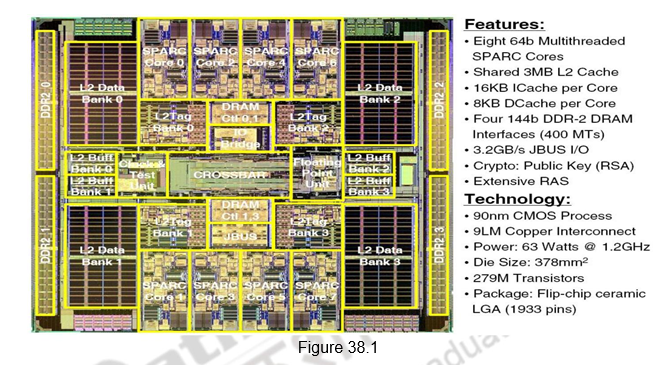
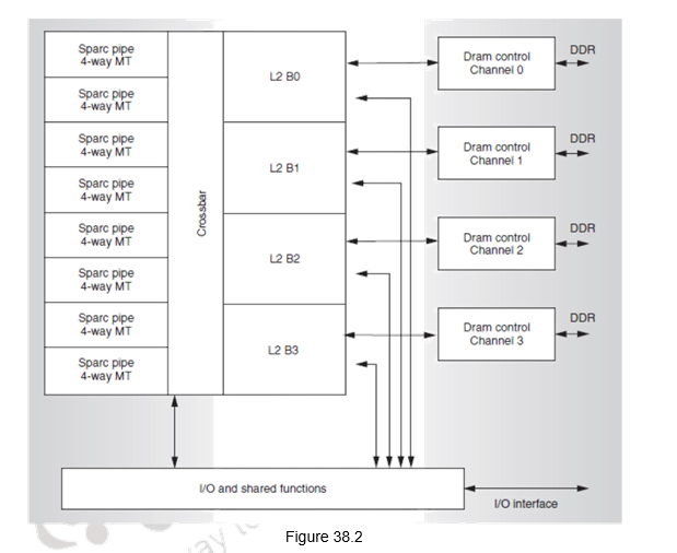
Niagara supports 32 threads of execution in hardware. The architecture organizes four threads into a thread group. The group shares a processing pipeline, referred to as the SPARC pipe. Niagara uses eight such thread groups, resulting in 32 threads on the CPU. Each SPARC pipe contains level-1 caches for instructions and data. The hardware hides memory and pipeline stalls on a given thread by scheduling the other threads in the group onto the SPARC pipe with a zero cycle switch penalty. The 32 threads share a 3-Mbyte level-2 cache. This cache is 4-way banked and pipelined. It is 12-way set-associative to minimize conflict misses from the many threads. The crossbar interconnect provides the communication link between SPARC pipes, L2 cache banks, and other shared resources on the CPU. It provides more than 200 Gbytes/s of bandwidth. A two-entry queue is available for each source-destination pair, and it can queue up to 96 transactions each way in the crossbar. The crossbar also provides a port for communication with the I/O subsystem. The crossbar is also the point of memory ordering for the machine. The memory interface is four channels of dual-data rate 2 (DDR2) DRAM, supporting a maximum bandwidth in excess of 20 Gbytes/s, and a capacity of up to 128 Gbytes. Figure 38.2 shows a block diagram of the Niagara processor.
SPARC Pipeline: The SPARC pipeline is a simple and straight forward pipeline consisting of six stages. Figure 38.3 shows the SPARC pipeline. Each SPARC pipeline supports four threads. Each thread has a unique set of registers and instruction and store buffers. The thread group shares the L1 caches, translation look -aside buffers (TLBs), execution units, and most pipeline registers. The pipeline consists of the six stages – fetch, thread select, decode, execute, memory, and write back. In the fetch stage, the instruction cache and instruction TLB (ITLB) are accessed. The following stage completes the cache access by selecting the way. The critical path is set by the 64-entry, fully associative ITLB access. A thread-select multiplexer determines which of the four thread program counters (PC) should perform the access. The pipeline fetches two instructions each cycle. A predecode bit in the cache indicates long -latency instructions.
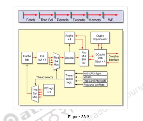
In the thread-select stage, the thread-select multiplexer chooses a thread from the available pool to issue an instruction into the downstream stages. This stage also maintains the instruction buffers. Instructions fetched from the cache in the fetch stage can be inserted into the instruction buffer for that thread if the downstream stages are not available. The thread-select logic decides which thread is active in a given cycle in the fetch and thread-select stages. As Figure 38.3 shows, the thread-select signals are common to fetch and thread-select stages. Therefore, if the thread -select stage chooses a thread to issue an instruction to the decode stage, the fetch stage also selects the same instruction to access the cache. The thread-select logic uses information from various pipeline stages to decide when to select or deselect a thread. For example, the thread-select stage can determine instruction type using a predecode bit in the instruction cache, while some traps are only detectable in later pipeline stages. Therefore, instruction type can cause deselection of a thread in the thread-select stage, while a late trap detected in the memory stage needs to flush a ll younger instructions from the thread and deselect itself during trap processing. Pipeline registers for the first two stages are replicated for each thread.
For single-cycle instructions such as ADD, Niagara implements full bypassing to younger instructions from the same thread to resolve RAW dependencies. Load instructions have a three-cycle latency before the results of the load are visible to the next instruction. Such long-latency instructions can cause pipeline hazards and resolving them requires stalling the corresponding thread until the hazard clears. So, in the case of a load, the next instruction from the same thread waits for two cycles for the hazards to clear.
In a multithreaded pipeline, threads competing for shared resources also encounter structural hazards. Resources such as the ALU that have a one-instruction-per-cycle throughput present no hazards, but the divider, which has a throughput of less than one instruction per cycle, presents a scheduling problem. In this case, any thread that must execute a DIV instruction has to wait until the divider is free. The thread scheduler guarantees fairness in accessing the divider by giving priority to the least recently executed thread. Although the divider is in use, other threads can use free resources such as the ALU, load-store unit, and so on.
The thread selection policy is to switch between available threads every cycle, giving priority to the least recently used thread. Threads can become unavailable because of long-latency instructions such as loads, branches, and multiply and divide. They also become unavailable because of pipeline stalls such as cache misses, traps, and resource conflicts. The thread scheduler assumes that loads are cache hits, and can therefore issue a dependent instruction from the same thread speculatively. However, such a speculative thread is assigned a lower priority for instruction issue as compared to a thread that can issue a non-speculative instruction.
Instructions from the selected thread go into the decode stage, which performs instruction decode and register file access. The supported execution units include an arithmetic logic unit (ALU), shifter, multiplier, and a divider. A bypass unit handles instruction results that must be passed to dependent instructions before the register file is updated. ALU and shift instructions have single cycle latency and generate results in the execute stage. Multiply and divide operations are long latency and cause a thread switch.
The load store unit contains the data TLB (DTLB), data cache, and store buffers. The DTLB and data cache access take place in the memory stage. Like the fetch stage, the critical path is set by the 64-entry, fully associative DTLB access. The load-store unit contains four 8-entry store buffers, one per thread. Checking the physical tags in the store buffer can indicate read after write (RAW) hazards between loads and stores. The store buffer supports the bypassing of data to a load to resolve RAW hazards. The store buffer tag check happens after the TLB access in the early part of write back stage.
Load data is available for bypass to dependent instructions late in the write back stage. Single-cycle instructions such as ADD will update the register file in the write back stage.
The L1 instruction cache is 16 Kbyte, 4-way set-associative with a block size of 32 bytes. A random replacement scheme is implemented for area savings, without incurring significant performance cost. The instruction cache fetches two instructions each cycle. If the second instruction is useful, the instruction cache has a free slot, which the pipeline can use to handle a line fill without stalling. The L1 data cache is 8 Kbytes, 4-way set-associative with a line size of 16 bytes, and implements a write-through policy. Even though the L1 caches are small, they significantly reduce the average memory access time per thread with miss rates in the range of 10 percent. Because commercial server applications tend to have large working sets, the L1 caches must be much larger to achieve significantly lower miss rates, so this sort of tradeoff is not favorable for area. However, the four threads in a thread group effectively hide the latencies from L1 and L2 misses. Therefore, the cache sizes are a good trade -off between miss rates, area, and the ability of other threads in the group to hide latency.
Niagara uses a simple cache coherence protocol. The L1 caches are write through, with allocate on load and no -allocate on stores. L1 lines are either in valid or invalid states. The L2 cache maintains a directory that shadows the L1 tags. The L2 cache also interleaves data across banks at a 64-byte granularity. A load that missed in an L1 cache (load miss) is delivered to the source bank of the L2 cache along with its replacement way from the L1 cache. There, the load miss address is entered in the corresponding L1 tag location of the directory, the L2 cache is accessed to get the missing line and data is then returned to the L1 cache. The directory thus maintains a sharers list at L1-line granularity. A subsequent store from a different or same L1 cache will look up the directory and queue up invalidates to the L1 caches that have the line. Stores do not update the local caches until they have updated the L2 cache. During this time, the store can pass data to the same thread but not to other threads; therefore, a store attains global visibility in the L2 cache. The crossbar establishes memory order between transactions from the same and different L2 banks, and guarantees delivery of transactions to L1 caches in the same order. The L2 cache follows a copy-back policy, writing back dirty evicts and dropping clean evicts. Direct memory accesses from I/O devices are ordered through the L2 cache. Four channels of DDR2 DRAM provide in excess of 20 Gbytes/s of memory bandwidth.
Each SPARC core has the following units:
• Instruction fetch unit (IFU) includes the following pipeline stages – fetch, thread selection, and decode. The IFU also includes an instruction cache complex.
• Execution unit (EXU) includes the execute stage of the pipeline.
• Load/store unit (LSU) includes memory and write-back stages, and a data cache complex.
• Trap logic unit (TLU) includes trap logic and trap program counters.
• Stream processing unit (SPU) is used for modular arithmetic functions for crypto.
• Memory management unit (MMU).
• Floating-point front end unit (FFU) interfaces to the FPU.
Thus, we see from the above details that the Niagara processor implements a thread-rich architecture designed to provide a high-performance solution for commercial server applications. The hardware supports 32 threads with a memory subsystem consisting of an on-board crossbar, level-2 cache, and memory controllers for a highly integrated design that exploits the thread-level parallelism inherent to server applications, while targeting low levels of power consumption.
Next, we shall discuss about IBM’s Cell Broad Band Engine (Cell BE) architecture.
IBM’s Cell BE: The Cell BE is a heterogeneous architecture developed by IBM, SCEI/Sony and Toshiba with the following design goals:
· An accelerator extension to Power o Built on a Power ecosystem
o Use best known system practices for processor design
· Setting a new performance standard
o Exploit parallelism while achieving high frequency
o Supercomputer attributes with extreme floating point capabilities
o Sustain high memory bandwidth
· Design for natural human interaction
o Photo-realistic effects
o Predictable real-time response
o Virtualized resources for concurrent activities
· Design for flexibility
o Wide variety of application domains
o Highly abstracted to highly exploitable programming models o Reconfigurable I/O interfaces
o Virtual trusted computing environment for security
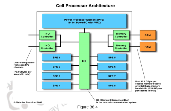
The Cell BE is a heterogeneous architecture because it has different types of cores. The Cell BE logically defines four separate types of functional components: the PowerPC Processor Element – one core (PPE), synergistic processor units – eight cores (SPU), the memory flow controller (MFC), and the internal interrupt controller (IIC). The computational units in the CBEA-compliant processor are the PPEs and the SPUs. Each SPU has a dedicated local storage, a dedicated MFC with its associated memory management unit (MMU), and a replacement management table (RMT). The combination of these components is called a Synergistic Processor Element (SPE). Figure 38.4 shows the architecture of Cell BE. The element interconnect bus (EIB) connects the various units within the processor.
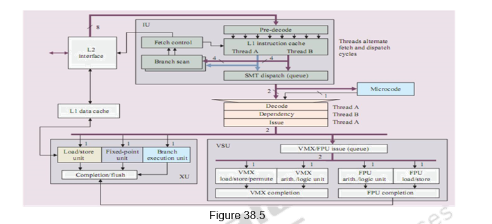
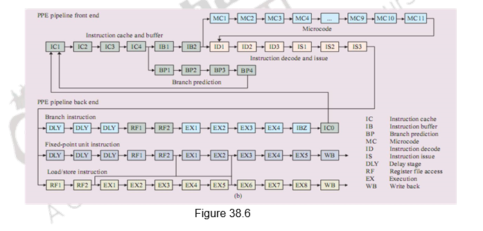
Power Processing Element: The PPE is a 64 bit, “Power Architecture” processor, with a 32KB primary instruction cache, a 32KB primary data cache and a 512KB secondary cache. It is a dual issue processor that is dual threaded with in-order static issue. It acts as the control unit for the SPEs. It runs the OS and most of the applications but compute intensive parts of the OS and applications will be offloaded to the SPEs. It is a RISC architecture that uses considerably less power than other PowerPC devices, even at higher clock rates. The major functional units of the PPE are given in Figure 38.5. It is composed of three main units – the Instruction Unit (IU), which takes care of the fetch, decode, branch, issue and completion, the Fixed-Point Execution Unit (XU), which handles the fixed – point instructions and load/store instructions and the Vector Scalar Unit (VSU), which handles the vector and floating point instructions. The PPE pipeline is illustrated in Figure 38.6.
Synergistic Processing Elements (SPEs): The SPEs are eight in number. They follow SIMD style instruction set architecture and are optimized for power and performance of computational-intensive applications. The various functional units of the SPE are shown in Figure 38.7 and the SPE pipeline is indicated in Figure 38.8. An SPE can operate on sixteen 8-bit integers, eight 16-bit integers, four 32-bit integers, or four single-precision floating-point numbers in a single clock cycle, as well as a memory operation.
The SPEs have a local store memory for instructions and data. This 256KB local store is the largest component of the SPE and acts as an additional level of memory hierarchy. It is a single-port SRAM, capable of reading and writing through both narrow 128-bit and wide 128-byte ports. The SPEs operate on registers which are read from or written to the local stores. The local stores can access main memory in blocks of 1KB minimum (16KB maximum) but the SPEs cannot act directly on main memory (they can only move data to or from the local stores). Caches can deliver similar or even faster data rates but only in very short bursts (a couple of hundred cycles at best), the local stores can each deliver data at this rate continually for over ten thousand cycles without going to RAM.
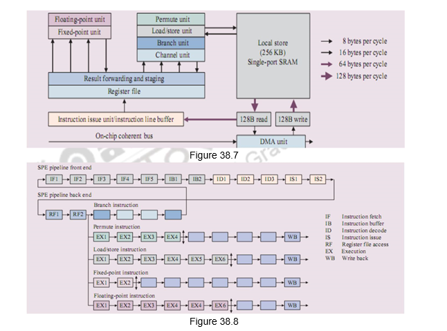
Data and instructions are transferred between the local store and the system memory by asynchronous DMA commands, controlled by the Memory Flow Controller, which provides support for 16 simultaneous DMA commands. The SPE instructions insert DMA commands into queues which are then pooled as DMA commands into a single “DMA list” command. They support a 128 entry unified register file for improved memory bandwidth, and optimum power efficiency and performance .
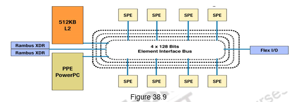
The Element Interconnect Bus (EIB) provides the data ring for internal communication. You can form four 16 byte data rings of low latency, multiple simultaneous transfers at 96B/cycle peak bandwidth (at ½ CPU speed). The EIB is shown in Figure 38.9.
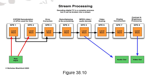
A big difference in Cells from normal CPUs is the ability of the SPEs in a Cell to be chained together to act as a stream processor. In one typical usage scenario, the system will load the SPEs with small programs , chaining the SPEs together to handle each step in a complex operation. For instance, the decoding of digital TV is a complex process that can be broken into a stream, as shown in Figure 38.10. The data would be passed off from SPE to SPE until the final processing is done. Another possibility is to partition the input data set and have several SPEs performing the same kind of operation in parallel. At 3.2 GHz, each SPE gives a theoretical 25.6 GFLOPS of single precision performance.
In order to deliver a significant increase in application performance in a power constrained environment, the Cell BE design exploits parallelism at all levels.
- Data level parallelism – with the SPEs and SIMD instruction support
- ILP – using a static scheduled and power aware micro-architecture
- Compute-transfer parallelism – using programmable data transfer engines
- TLP – with a multicore design approach and hardware multithreading on the PPE
- Memory level parallelism – by overlapping transfers from multiple requests per core and from multiple cores
Thus, the Cell BE was designed based on the analysis of a broad range of workloads in areas such as cryptography, graphics transforms and lighting, physics, fast-Fourier transforms (FFT), matrix operations, and scientific workloads and is designed for graphics- and network-intensive jobs ranging from video games to complex imaging for the medical, defense, automotive and aerospace industries.
To summarize, we have dealt with two different styles of multicore architectures in this module:
- UltraSPARC
– Homogeneous
– Multithreaded
– Server applications
– Power efficient
- IBM’s Cell BE
– Heterogeneous
– Built for gaming applications
– Exploits different types of parallelism
Web Links / Supporting Materials
- Computer Architecture – A Quantitative Approach , John L. Hennessy and David A. Patterson, 5th Edition, Morgan Kaufmann, Elsevier, 2011.
- IBM, Sony, Toshiba papers in ISSCC’05
- “A Streaming Processing Unit for a CELL Processor”, B. Flachs et. al.
- “The Design and Implementation of a First-Generation CELL Processor”, D. Pham et. al.
- “Microprocessor Report”,
- Reed Electronics Group, 2005, Jan. 31 & Feb. 14
- “IBM’s Cell Processor : The next generation of computing?”, D.K. Every, Shareware Press, Feb. 2005
- “Power Efficient Processor Architecture and The Cell Processor”, H.P. Hofstee, HPCA-11 2005
- “Power Efficient Processor Design and the Cell Processor”, IBM, 2005
- “Introducing the IBM/Sony/Toshiba Cell Processor”, J. H. Stokes, http://arstechnica.com/
- “Cell Architecture Explained”, N. Blachford, http://www.blachford.info/
- Kunle Olukotun, Poonacha Kongetira, Kathirgamar Aingaran, “Niagara: A 32-Way Multithreaded Sparc Processor”, IEEE Micro, vol. 25, no. , pp. 21-29, March/April 2005, doi:10.1109/MM.2005.35