32 Exploiting Data Level Parallelism
Dr A. P. Shanthi
The objectives of this module are to discuss about how data level parallelism is exploited in processors. We shall discuss about vector architectures, SIMD instructions and Graphics Processing Unit (GPU) architectures.
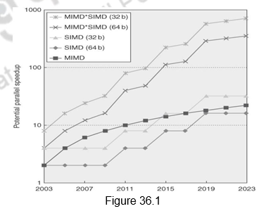
We have discussed different techniques for exploiting instruction level parallelism and thread level parallelism in our earlier modules. We shall now discuss different types of architectures that exploit data level parallelism, i.e. SIMD style of architectures. SIMD architectures can exploit significant data-level parallelism for not only matrix-oriented scientific computing, but also for media-oriented image and sound processing, which are very popular these days. Additionally, SIMD is more energy efficient than MIMD, as we need to fetch only one instruction per data operation. This makes SIMD attractive for personal mobile devices also. Figure 36.1 shows the potential speedup via parallelism from MIMD, SIMD, and both MIMD and SIMD over time for x86 computers. This figure assumes that two cores per chip for MIMD will be added every two years and the number of operations for SIMD type of computing will double every four years. The potential speedup from SIMD is expected to be twice that from MIMD. Therefore, it is essential that we discuss the details of SIMD architectures.
There are basically three variations of SIMD. They are:
• Vector architectures
• SIMD extensions
• Graphics Processor Units (GPUs) We shall discuss each of these in detail.
Vector Architectures: This is the oldest of the SIMD style of architectures, widely used in the super computers of those days. They were considered too expensive to be implemented in microprocessors because of the number of transistors required and the memory bandwidth required. However, it is no longer so. Vector architectures basically operate on vectors of data. They gather data that is scattered across multiple memory locations into one large vector register, operate on the data elements independently and then store back the data in the respective memory locations. These large register files are controlled by compiler and are used to hide memory latency and to leverage the memory bandwidth.
As an example architecture, in order to understand the concepts of a vector processor, we will look at the VMIPS architecture, whose scalar version is the MIPS architecture, that we are already familiar with. The primary components of the VMIPS ISA are as shown in Figure 36.2. They are the following:
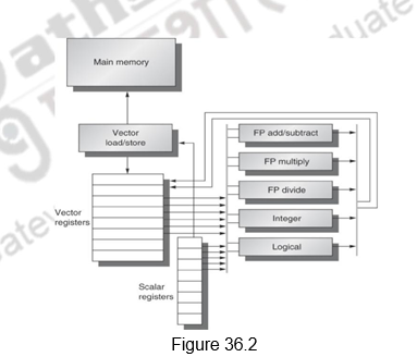
1. Vector registers: Each of these registers holds a vector. In the case of the VMIPS architecture, there are eight registers and each register holds a 64-element, 64 bits/element vector. In order to supply data to the functional units and provide enough overlap, the register file has 16 read ports and 8 write ports , connected to the inputs or outputs of the functional units through crossbar switches.
2. Vector functional units: These functional units are fully pipelined, capable of starting an operation every clock cycle. A control unit detects the structural hazards and data hazards. There are five functional units indicated in the figure.
3. Vector load-store unit: This unit handles the vector data to be loaded from and to memory. They are fully pipelined units, with a bandwidth of one word per clock cycle, after the initial latency. This unit also handles scalar loads and stores.
4. Scalar registers: These registers can pass on inputs to the vector functional units and also compute the addresses for the vector load/store operations. There are 32 general-purpose registers and 32 floating-point registers. One input of the vector functional units latches scalar values as they are read out of the scalar register file.
5. The ISA of VMIPS consists of vector instructions, in addition to the scalar instructions of MIPS. For example, the ADDVV.D instruction adds two vectors, ADDVS.D adds a vector to a scalar and LV/SV performs vector load and vector store from the starting address indicated in the MIPS general purpose register. Apart from these, there are also two general purpose registers, the vector length register to be used when the vector length is different and the vector mask register to be used with conditional execution.
To give a clearer picture of the vector operations, consider the following code sequence to perform the operation Y = a * X + Y.
DAXPY (double precision a*X+Y)
L.D F0, a; load scalar a
LV V1, Rx; load vector X
MULVS.D V2, V1, F0; vector-scalar multiply
LV V3, Ry; load vector Y
ADDVV V4, V2, V3; add
SV Ry, V4; store the result
The corresponding MIPS code is shown below.
L.D F0, a ; load scalar a
DADDIUR4, Rx, #512; last address to load
Loop: L.D F2, 0(Rx); load X[i]
MUL.D F2, F2, F0; a x X[i]
L.D F4,0(Ry); load Y[i]
ADD.D F4, F2, F2; a x X[i] + Y[i]
S.D F4, 9(Ry); store into Y[i]
DADDIU Rx, Rx, #8; increment index to X
DADDIU Ry, Ry, #8; increment index to Y
SUBBU R20, R4, Rx; compute bound
BNEZ R20, Loop; check if done
It can be easily seen that VMIPS requires only 6 instructions, whereas, MIPS takes about 600 instructions. This is because of the vector operations done (which would have otherwise been done in an iterative manner) and the removal of the loop overhead instructions. Another important difference is the frequency of interlocks. In the case of the MIPS code, the dependences will cause stalls, whereas, in the case of VMIPS, each vector instruction will stall only for the first vector element. Thus, pipeline stalls will occur only once per vector instruction, rather than vector element. Although loop unrolling and software pipelining can help reduce the stalls in MIPS, there will not be a significant reduction.
Vector Execution Time: The vector execution time depends on three factors
– Length of operand vectors
– Structural hazards
– Data dependences
Given the length of the vector and the initiation rate, which is the rate at which a vector unit consumes new operands and produces new results, we can calculate the time taken to execute a vector instruction. With just one lane and the initiation rate of one element per clock cycle, the execution time for one vector instruction is approximately the vector length. We normally talk about convoys, which is the set of vector instructions that could execute together. We define chime as the unit of time to execute one convoy. So, m convoys execute in m chimes, and if the vector length is n, it takes m x n clock cycles to execute. Look at the following code sequence:
LV V1, Rx; load vector X
MULVS.D V2,V1,F0 ;vector-scalar
LV V3,Ry ; load vector Y
ADDVV.D V4,V2,V3 ; add two vectors
SV Ry, V4 ; store the sum
There are three convoys and so 3 chimes, with 2 floating point operations per result. Therefore, the cycles per FLOP = 1.5. For 64 element vectors, it requires 64 x 3 = 192 clock cycles. Of-course, we are assuming that sequences with read-after-write dependency hazards can be in the same convoy via chaining. Chaining allows a vector operation to start as soon as the individual elements of its vector source operand become available. For example, as the first vector element gets loaded from memory, it is chained to the multiplier unit. Similarly, the output of the second load and the multiply are chained to the adder unit. The most important overhead ignored by the chime model discussed here, is the vector start up time, which depends on the latency of the vector functional unit.
Improving the Performance of Vector Processors: Having discussed the basics of a vector architecture, we will now look at methods that are normally adopted by vector architectures to improve performance. The following optimizations are normally done.
Multiple Lanes: This optimization looks at having parallel lanes so that more than one element is generated per clock cycle. Figure 36.3 shows how multiple lanes can be used. The processor on the left has only one lane (one add pipeline) and produces only one addition per clock cycle. The one on the right has four lanes and produces four additions per clock cycle. The elements of the vector are interleaved across the multiple lanes.
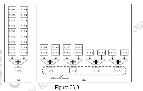
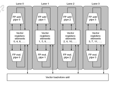
Figure 36.4
Figure 36.4 shows how the four lanes are formed. The vector register storage is divided among the four lanes, with each lane holding every fourth element of the vector register. The adder unit, the multiplier unit and the load/store unit work together on four parallel lanes. The arithmetic units have four execution pipelines. Adding multiple lanes is a popular way of increasing the performance of vector processors as it does not increase the control and design complexity too much.
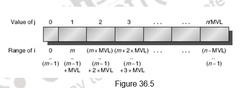
Vector Length Registers to handle non-64 wide vectors: The natural vector length depends on the length of the vector registers. In our case, it is 64. But, this may not be true always and the length may not even be known at compile time. Therefore, processors look at the usage of Vector Length Register (VLR). The length of the vector can be loaded into this register. This will work as long as the real length is less than the maximum vector length, which the vector register length. In cases where the real leng th is greater than the maximum length, the technique of strip mining is used. Here, several iterations that are multiples of the maximum length are done and the remaining iterations are done separately. Figure 36.5 illustrates the idea.
Vector Mask Registers to handle IF statements in vector code: Sometimes, we may not want to execute the operation on all the elements of the vector. Depending on some condition, we may want to operate on certain elements alone. This is done with the help of a vector mask register, which has one bit per element. Depending on whether the masking bit is set or not for each element, the operation is carried out for that element.
Memory Banks – Memory system optimizations to support vector processors : As the memory bandwidth demands are very high for vector processors, memory interleaving and independent memory banks are used. Support for controlling the bank addresses independently, Loading or storing non sequential words and multiple vector processors sharing the same memory are provided.
Stride: Handling Multiple Dimensional Matrices in Vector Processors: Strided addressing skips a fixed number of words between each access, so that data is accessed with non-unit strides and stored in a vector register. Sequential addressing is often called unit stride addressing. Once the accessing is done with a different stride length and stored in the register, the operations on these elements are carried out in the usual manner.
Scatter-Gather: To Handle Sparse matrices: Many a times we need to handle sparse data. Gather and scatter operations help collecting the data and then storing them back using index vectors. A gather operation takes an index vector and fetches the vector whose elements are at the addresses given by adding a base address to the offsets given in the index vector. After performing the operations on these elements in a dense form, the sparse vector can be stored in an expanded form using the same index vector.
Programming Vector Architectures: Program structures affecting performance: An advantage of this architecture is that it provides a simple execution model and the compiler can tell the programmer which portions have been vectorized and which have not been. The compilers can provide feedback to programmers and the programmers can provide hints to the compiler. This transparency makes improvement possible. Of-course, a lot depends on the program structure itself – dependences, the algorithms chosen and how they are coded.
SIMD Instruction Set Extensions: SIMD multimedia extensions started with the simple observation that many media applications operate on data types that have narrower widths than the native word size. For example, an adder can be partitioned into smaller sized adders. However, unlike the vector instructions which are very elegant, the SIMD extensions have the following limitations, compared to vector instructions:
1. The number of data operands are encoded into the op code itself and so the number of instructions increases tremendously. There is no usage of a vector length register.
2. There is no support for sophisticated addressing modes for example for strided accesses and scatter-gather accesses.
3. There is no support for conditional execution as there is no support for masking registers.
4. All these makes it harder for the compiler to generate SIMD code and increases the difficulty of programming in SIMD assembly language
The following are the SIMD extensions that have been implemented:
- Intel MMX (1996)
- Eight 8-bit integer ops or four 16-bit integer ops
- Streaming SIMD Extensions (SSE) (1999)
- Eight 16-bit integer ops
- Four 32-bit integer/fp ops or two 64-bit integer/fp ops
- Advanced Vector Extensions (2010)
- Four 64-bit integer/fp ops
- Operands must be consecutive and aligned memory location
- Generally designed to accelerate carefully written libraries rather than for compilers
In-spite of the disadvantages, SIMD extensions have certain advantages over the vector architectures:
- It costs little to add to the standard ALU and it is easy to implement
- It requires little extra state, which means it is also easy for context-switch o It requires little extra memory bandwidth
- There is no virtual memory problem of cross -page access and page-fault
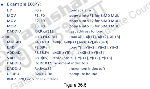
Figure 36.6 shows the code for the DXPY loop using the SIMD extension instructions.
Graphics Processing Units (GPUs): The third style of architecture that exploits data level parallelism is the GPU. GPUs, with their highly parallel operations, have become very popular for media applications. This, combined with the availability of a programming language to program the GPUs has opened up the option of using GPUs for general purpose computing.
GPUs support a heterogeneous execution model, with the CPU as the host and the GPU as the device. The challenge lies in partitioning the computations between the CPU and the GPU and the usage of the system memory/device memory. GPUs have every type of parallelism that can be captured by the programming environment – MIMD, SIMD, multithreading and ILP.
NVIDIA has developed a C like language to exploit all sorts of parallelism and make the programming of GPUs easy through their Compute Unified Device Architecture (CUDA). OpenCL is a vendor independent programming language for multiple platforms. All this has made the programming of GPUs easier and the increased popularity of GP-GPU Computing.
NVIDIA has unified all forms of GPU parallelism as a CUDA thread. The compiler and the hardware can together combine thousands of such threads to exploit all forms of parallelism. The programming model is “Single Instruction Multiple Thread”. A thread is associated with each data element. Threads are organized into blocks. We can have Thread Blocks of up to 512 elements. A Multithreaded SIMD Processor is the hardware that executes a whole thread block (32 elements executed per thread at a time) . The thread blocks are organized into a grid and blocks are executed independently and in any order. Different blocks cannot communicate directly but can coordinate using atomic memory operations in Global Memory. The GPU hardware itself handles the thread management, rather than the applications or OS. A multiprocessor is composed of multithreaded SIMD processors. A Thread Block Scheduler is responsible for scheduling the threads.
A GPU architecture is similar to vector architectures in that they work well with data-level parallel problems, have support for scatter-gather transfers, have support for mask registers and have large register files. The differences are that they do not have a scalar processor, use multithreading to hide memory latency and have many functional units, as opposed to a few deeply pipelined units .
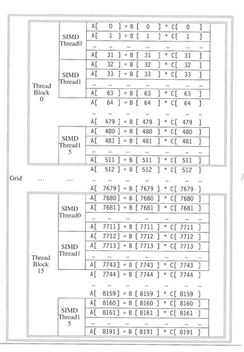
As an example, let us consider the multiplication of two vectors of length 8192. The code that works over all the 8192 elements is the grid. The thread blocks break this down into manageable sizes, say, 512 elements / block. So, we have 16 SIMD threads / block, with 32 elements / thread. An SIMD instruction executes 32 elements at a time . Therefore, the grid size is 16 blocks, where a block is analogous to a strip-mined vector loop with vector length of 32. A block is assigned to a multithreaded SIMD processor by the thread block scheduler. The thread scheduler uses scoreboard to dispatch and there should not be any data dependencies between threads. The number of multithreaded SIMD processors varies for various GPUS. The c urrent-generation GPUs like Fermi have 7-15 multithreaded SIMD processors. This mapping is illustrated in Figure 36.7. Within each SIMD processor, there are 32 SIMD lanes, which are wide and shallow compared to vector processors. From the programmer’s perspective, a kernel is a sequence of instructions that can be executed in parallel, a thread is a basic unit of execution that executes a single kernel, a thread block is a collection of threads that execute the same kernel and a grid is a collection of thread blocks that execute the same kernel. A CUDA program can start many grids, one for each parallel task required.
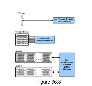
GPU Memory Structures: There are different memories that are supported in a GPU architecture. Each SIMD lane has a private section of off-chip DRAM, called the private memory, which is used to contain stack frames, spilling registers, and private variables. Each multithreaded SIMD processor also has a local memory, which is shared by SIMD lanes / threads within a block. The memory shared by all the SIMD processors is the GPU memory and the host can read and write GPU memory. Figure 36.8 shows the memory hierarchy of the CUDA threads.
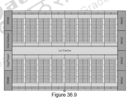
Fermi Architecture Case Study: Figure 36.9 shows the floor plan of the Fermi GTX 480 GPU. There are 16 multithreaded SIMD Processors. The Thread Block Scheduler is highlighted on the left. The GTX 480 has 6 GDDR5 ports, each 64 bits wide, supporting up to 6 GB of capacity. The Host Interface is PCI Express 2.0 x 16. Giga Thread is the name of the scheduler that distributes thread blocks to Multiprocessors, each of which has its own SIMD Thread Scheduler.
NVIDIA engineers analyzed hundreds of shader programs that showed an increasing use of scalar computations and realized it’s hard to efficiently utilize all processing units with a vector architecture. They also estimated that as much as 2× performance improvement can be realized from a scalar architecture that uses 128 scalar processors versus one that uses 32 four-component vector processors, based on architectural efficiency of the scalar design. So starting from G80, NVIDIA moved to a scalar processor based design.
A CUDA Core, shown in Figure 36.10 is a simple scalar processor that has a fully pipelined Arithmetic Logic Unit (ALU) and a Floating Point Unit (FPU). It executes a single floating point or integer instruction per clock. It has a very simple instruction pipeline. The Fermi architecture consists of 512 CUDA cores. A Streaming Multi-Processor (SM) is a collection of 32 CUDA cores that share the same L1 cache. The 32 CUDA cores are further divided into two sets of 16 cores. There are 16 load/store units that can access data from the cache/DRAM. The 4 Special Function Units (SFUs) execute complex instructions like sin, cosine, reciprocal, square root etc.
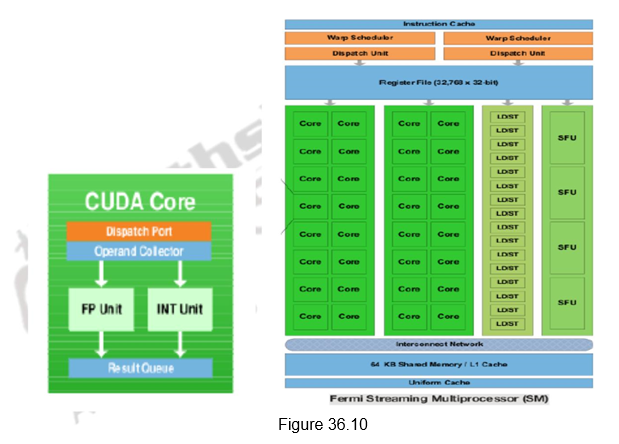
Fermi supports a two-level scheduler. At the chip level, a global scheduler schedules thread blocks to various SMs, while at the SM level, a warp scheduler distributes warps of 32 threads to its execution units. Fermi supports concurrent kernel execution, where different kernels of the same application context can execute on the GPU at the same time. Concurrent kernel execution allows programs that execute a number of small kernels to utilize the whole GPU. The SM schedules threads in groups of 16 parallel threads called warps. Each SM features two warp schedulers and two instruction dispatch units, allowing two warps to be issued and executed concurrently. Fermi’s dual warp scheduler selects two warps, and issues one instruction from each warp to a group of sixteen cores, sixteen load/store units, or four SFUs.
The per-SM L1 cache is configurable to support both shared memory and caching of local and global memory operations. The 64 KB memory can be configured as either 48 KB of Shared memory with 16 KB of L1 cache, or 16 KB of Shared memory with 48 KB of L1 cache. When configured with 48 KB of shared memory, programs that make extensive use of shared memory (such as electro-dynamic simulations) can perform up to three times faster. For programs whose memory accesses are not known beforehand, the 48 KB L1 cache configuration offers greatly improved performance over direct access to DRAM. The innovations in the Fermi architecture include fast double precision, caches for GPU memory, 64-bit addressing and unified address space, support for error correcting codes, faster context switching and faster atomic instructions.
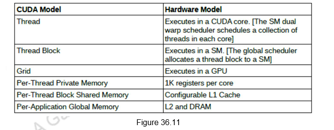
The CUDA programming model, involving threads, thread blocks and grids, map directly to the Fermi hardware architecture, involving CUDA cores, SM’s and the whole GPU. This is shown in Figure 36.11.
NVIDIA GPU ISA: The instruction set target of the NVIDIA compilers is an abstraction of the hardware instruction set. Parallel Thread Execution (P TX) is a low level virtual machine and ISA designed to support the operations of a parallel thread processor. It provides a stable instruction set for the compilers and is compatible across generations of GPU architectures. The hardware instruction set is hidden from the programmer. PTX instructions describe the operations on a single CUDA thread, and generally map to the hardware instructions. Also, one PTX can map to multiple instructions and vice versa. At program install time, PTX instructions are translated to machine instructions by the GPU driver.
Summary:
The salient points of this module are summarized below:
- Data level parallelism that is present in applications is exploited by vector architectures, SIMD style of architectures or SIMD extensions and Graphics Processing Units.
- Vector architectures support vector registers, vector instructions, deeply pipelined functional units and pipelined memory access.
- Special features like conditional execution, varying lengths of vector, scatter-gather operations, chaining, etc. are supported in vector processors.
- SIMD extensions in processors exploit DLP with minimal changes to the hardware.
- They are very useful for streaming applications.
- GPUs try to exploit all types of parallelism and form a heterogeneous architecture.
- There are multiple SIMD lanes with multithreaded execution.
- The memory hierarchy supports efficient access of data.
- There is support for PTX low level virtual machine execution.
- Fermi architecture was done as a case study of the GPU architecture.
Web Links / Supporting Materials
- Computer Architecture – A Quantitative Approach , John L. Hennessy and David A. Patterson, 5th Edition, Morgan Kaufmann, Elsevier, 2011.
- NVIDIA White Papers:
- http://www.nvidia.in/content/PDF/fermi_white_papers/NVIDIA_Fermi_Compute_Architecture_Whitepaper.pdf